ESD5B5.0ST1G ON Semiconductor, ESD5B5.0ST1G Datasheet
ESD5B5.0ST1G
Specifications of ESD5B5.0ST1G
ESD5B5.0ST1GOSTR
Available stocks


Related parts for ESD5B5.0ST1G

ESD5B5.0ST1G Summary of contents
Page 1
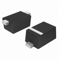
... Code orientation and/or position may vary depending upon manufacturing location. ORDERING INFORMATION Device Package Shipping ESD5B5.0ST1G SOD-523 3000/Tape & Reel (Pb-Free) †For information on tape and reel specifications, including part orientation and tape sizes, please refer to our Tape and Reel Packaging Specifications Brochure, BRD8011/D ...
Page 2
... V is measured with a pulse test current For test procedure see Figures 3 and 4 and Application Note AND8307/D. Figure 1. ESD Clamping Voltage Screenshot Positive 8 kV Contact per IEC 61000-4-2 ESD5B5.0ST1G RWM (T = 25°C unless otherwise noted 0.9 V Max ...
Page 3
... IC will be exposed to during an ESD event to as low a voltage as possible. The ESD clamping voltage is the voltage drop across the ESD protection diode during an ESD event per the IEC61000-4-2 waveform. Since the IEC61000-4-2 was written as a pass/fail spec for larger ESD5B5.0ST1G IEC61000-4-2 Waveform I peak 100% ...
Page 4
... LITERATURE FULFILLMENT: Literature Distribution Center for ON Semiconductor P.O. Box 5163, Denver, Colorado 80217 USA Phone: 303-675-2175 or 800-344-3860 Toll Free USA/Canada Fax: 303-675-2176 or 800-344-3867 Toll Free USA/Canada Email: orderlit@onsemi.com ESD5B5.0ST1G PACKAGE DIMENSIONS SOD-523 CASE 502-01 ISSUE C NOTES: 1. DIMENSIONING AND TOLERANCING PER ANSI Y14.5M, -Y- 1982 ...