CD143A-SR2.8 Bourns Inc., CD143A-SR2.8 Datasheet

IC TVS ARRAY 2-LINE 2.8V SOT-143

CD143A-SR2.8

Manufacturer Part Number
CD143A-SR2.8
Description
IC TVS ARRAY 2-LINE 2.8V SOT-143
Manufacturer
Bourns Inc.
Datasheet

Specifications of CD143A-SR2.8

Package / Case
SOT-143, SOT-143B, TO-253AA
Voltage - Reverse Standoff (typ)
2.8V
Voltage - Breakdown
3V
Power (watts)
200W
Polarization
2 Channel Array - Unidirectional
Mounting Type
Surface Mount
Polarity
Unidirectional
Clamping Voltage
5 V
Operating Voltage
2.8 V
Breakdown Voltage
3 V
Termination Style
SMD/SMT
Peak Surge Current
30 A
Peak Pulse Power Dissipation
300 W
Capacitance
4.5 pF
Maximum Operating Temperature
+ 155 C
Minimum Operating Temperature
- 55 C
Dimensions
1.39 (Max) mm W x 3.04 (Max) mm L
Suppressor Type
Diode Arrays
Esd Protection Voltage
±30KV@Air Gap/±30KV@Contact Disc
Configuration
Dual
Mounting Style
Surface Mount
Clamping Voltage (max)
8.5VV
Working Voltage (max)
2.8VV
Leakage Current (max)
5uAA
Operating Temperature Min Deg. C
-55C
Operating Temperature Max Deg. C
125C
Product Length (mm)
3.04(Max)mm
Product Depth (mm)
1.39(Max)mm
Product Height (mm)
1.14(Max)mm
Pin Count
3 +Tab
Rad Hardened
No
Lead Free Status / RoHS Status
Lead free / RoHS Compliant
Lead Free Status / RoHS Status
Lead free / RoHS Compliant, Lead free / RoHS Compliant
Other names
CD143A-SR2.8TR
The CD143A-SR2.8 and CD143A-SR3.3 devices provides ESD
protection for the external ports of portable electronic devices such
as cell phones, handheld electronics and personal computers.
The ESD protection provided by the component enables a data
port to withstand a minimum ±8 KV Contact / ±15 KV Air Discharge
per the ESD test method specified in IEC 61000-4-2. The device
measures 2.80 mm x 1.20 mm and is available in a SOT-143
package intended to be mounted directly onto an FR4 printed
circuit board.
The Bourns
(EFT) and IEC 61000-4-5 (Surge) requirements.
Notes:
1. See Peak Pulse Power vs. Pulse Time.
2. From Pin 4 to Pin 1.
3. See Pulse Wave Form.
4. From Pin 1 to Pin 3, Pin 1 to Pin 2.
*No lead detected in standard tests of homogeneous materials.
**RoHS Directive 2002/95/EC Jan 27 2003 including Annex
Specifications are subject to change without notice.
Customers should verify actual device performance in their specific applications.
Absolute Maximum Ratings (@ T A = 25 °C Unless Otherwise Noted)
Electrical and Thermal Characteristics (@ T A = 25 °C Unless Otherwise Noted)
General Information
Parameter
Peak Pulse Power (t
Peak Pulse Current (t
Operating Supply Voltage (Vdd - Gnd)
ESD per IEC 61000-4-2
DC Voltage at any I/O Pin
Operating Temperature
Storage Temperature
Parameter
Breakdown Voltage Minimum @ 2 µA
Working Peak Voltage
Snap-Back Voltage Minimum @ 50 mA
Clamping Voltage Maximum @ I
Reverse Leakage Current Maximum @ V
Forward Voltage Maximum @ 15 mA
Leakage Current @ V
Capacitance Typical @ 0 V, 1 MHz
ESD Protection per IEC 61000-4-2
EFT Protection per IEC 61000-4-4 @ 5/50ns
Surge Protection per IEC 61000-4-5 @ 8/20µs
(Air)
(Contact)
Minimum Contact Discharge
Minimum Air Discharge
®
device will meet IEC 61000-4-2 (ESD), IEC 61000-4-4
p
p
= 8/20 µs)
WM
2
= 8/20 µs)
4
1
P
P
= 1 A
2,3
4
2
2,3
WM
2
CD143A-SR2.8~3.3 – Steering/TVS Diode Array Series
Features
Lead free as standard*
RoHS compliant**
ESD protection
Protects 2 lines
Low leakage current
Low capacitance
Symbol
Symbol
Surge
T
V
ESD
V
EFT
P
V
V
V
I
V
V
V
C
T
STG
V
I
PP
WM
I
esd
BR
SB
PP
dc
D
L
io
C
C
J
f
J
CD143A-SR2.8
8.5 @ 5 A
3.0
2.8
2.8
5.0
(Gnd - 0.50) to (Vdd + 0.5)
GND
I/O
-55 ˚C to 125 ˚C
-55 ˚C to 150 ˚C
+/-15
+/-8
5.0
1.0
1.0
4.5
1
2
40
12
Value
200
±30
3.8
12
Applications
Ethernet - 10/100/1000 Base T
Firewire and USB
Portable electronics
Video/Graphic Cards
CD143A-SR3.3
15 @ 10 A
3.5
3.3
3.3
7.0
4
3
REF
I/O
Unit
Unit
kV
uA
µA
pF
kV
˚C
˚C
W
A
A
A
V
V
V
V
V
V
V
V

Related parts for CD143A-SR2.8

CD143A-SR2.8 Summary of contents

Page 1

... General Information The CD143A-SR2.8 and CD143A-SR3.3 devices provides ESD protection for the external ports of portable electronic devices such as cell phones, handheld electronics and personal computers. The ESD protection provided by the component enables a data port to withstand a minimum ±8 KV Contact / ±15 KV Air Discharge per the ESD test method specified in IEC 61000-4-2 ...

Page 2

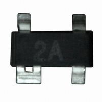
... CD143A-SR2.8~3.3 – Steering/TVS Diode Array Series Product Dimensions This is a molded JEDEC SOT-143 device. It weighs approximately 35 mg and has a flammability rating of UL 94V-0. The dimensions for the packaged device are shown below Recommended Pad Layout This is the footprint recommended for this SOT-143 device. ...

Page 3

... CD143A-SR2.8~3.3 – Steering/TVS Diode Array Series Performance Graphs Pulse Wave Form 120 Waveform Parameters µs 100 – Time (µs) Forward Clamping Voltage vs. Peak Pulse Current Waveform Parameters µ µ Peak Pulse Current (A) Typical Variation of C vs. V I/O-to-I/O IN 0.8 0.7 0.6 0.5 ...

Page 4

... CD143A-SR2.8~3.3 – Steering/TVS Diode Array Series Packaging Information The surface mount product is packaged tape and reel format per EIA-481 standard Index Hole Trailer Device ....... ....... ....... End ....... ....... 10 pitches (min.) Item Symbol Carrier Width A Carrier Length B Carrier Depth C Sprocket Hole d Reel Outside Diameter D Reel Inner Diameter ...

Related keywords