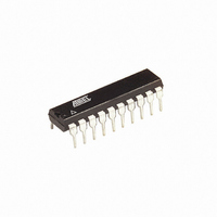
ATTINY2313-20PU Atmel, ATTINY2313-20PU Datasheet - Page 101

ATTINY2313-20PU
Manufacturer Part Number
ATTINY2313-20PU
Description
IC MCU AVR 2K FLASH 20DIP
Manufacturer
Atmel
Series
AVR® ATtinyr
Datasheets
1.ATTINY2313-20MU.pdf
(226 pages)
2.ATTINY2313V-10MU.pdf
(15 pages)
3.ATTINY2313V-10SU.pdf
(20 pages)
Specifications of ATTINY2313-20PU
Core Processor
AVR
Core Size
8-Bit
Speed
20MHz
Connectivity
SPI, UART/USART
Peripherals
Brown-out Detect/Reset, POR, PWM, WDT
Number Of I /o
18
Program Memory Size
2KB (1K x 16)
Program Memory Type
FLASH
Eeprom Size
128 x 8
Ram Size
128 x 8
Voltage - Supply (vcc/vdd)
2.7 V ~ 5.5 V
Oscillator Type
Internal
Operating Temperature
-40°C ~ 85°C
Package / Case
20-DIP (0.300", 7.62mm)
Package
20PDIP
Device Core
AVR
Family Name
ATtiny
Maximum Speed
20 MHz
Operating Supply Voltage
3.3|5 V
Data Bus Width
8 Bit
Number Of Programmable I/os
18
Interface Type
SPI/USART/USI
Number Of Timers
2
Processor Series
ATTINY2x
Core
AVR8
Data Ram Size
128 B
Maximum Clock Frequency
20 MHz
Maximum Operating Temperature
+ 85 C
Mounting Style
Through Hole
3rd Party Development Tools
EWAVR, EWAVR-BL
Development Tools By Supplier
ATAVRDRAGON, ATSTK500, ATSTK600, ATAVRISP2, ATAVRONEKIT
Minimum Operating Temperature
- 40 C
Cpu Family
ATtiny
Device Core Size
8b
Frequency (max)
20MHz
Total Internal Ram Size
128Byte
# I/os (max)
18
Number Of Timers - General Purpose
2
Operating Supply Voltage (typ)
3.3/5V
Operating Supply Voltage (max)
5.5V
Operating Supply Voltage (min)
2.7V
Instruction Set Architecture
RISC
Operating Temp Range
-40C to 85C
Operating Temperature Classification
Industrial
Mounting
Through Hole
Pin Count
20
Package Type
PDIP
For Use With
ATSTK600-DIP40 - STK600 SOCKET/ADAPTER 40-PDIP770-1007 - ISP 4PORT ATMEL AVR MCU SPI/JTAGATAVRDRAGON - KIT DRAGON 32KB FLASH MEM AVRATAVRISP2 - PROGRAMMER AVR IN SYSTEMATJTAGICE2 - AVR ON-CHIP D-BUG SYSTEM
Lead Free Status / RoHS Status
Lead free / RoHS Compliant
Data Converters
-
Lead Free Status / Rohs Status
Lead free / RoHS Compliant
Available stocks
Company
Part Number
Manufacturer
Quantity
Price
Part Number:
ATTINY2313-20PU
Manufacturer:
ATMEL/爱特梅尔
Quantity:
20 000
2543L–AVR–08/10
The Timer/Counter Overflow Flag (TOV1) is set at the same timer clock cycle as the OCR1x
Registers are updated with the double buffer value (at BOTTOM). When either OCR1A or ICR1
is used for defining the TOP value, the OCF1A or ICF1 flag set when TCNT1 has reached TOP.
The interrupt flags can then be used to generate an interrupt each time the counter reaches the
TOP or BOTTOM value.
When changing the TOP value the program must ensure that the new TOP value is higher or
equal to the value of all of the Compare Registers. If the TOP value is lower than any of the
Compare Registers, a compare match will never occur between the TCNT1 and the OCR1x.
As
in all periods. Since the OCR1x Registers are updated at BOTTOM, the length of the rising and
the falling slopes will always be equal. This gives symmetrical output pulses and is therefore fre-
quency correct.
Using the ICR1 Register for defining TOP works well when using fixed TOP values. By using
ICR1, the OCR1A Register is free to be used for generating a PWM output on OC1A. However,
if the base PWM frequency is actively changed by changing the TOP value, using the OCR1A as
TOP is clearly a better choice due to its double buffer feature.
In phase and frequency correct PWM mode, the compare units allow generation of PWM wave-
forms on the OC1x pins. Setting the COM1x1:0 bits to two will produce a non-inverted PWM and
an inverted PWM output can be generated by setting the COM1x1:0 to three (See
page
port pin is set as output (DDR_OCF1x). The PWM waveform is generated by setting (or clearing)
the OCF1x Register at the compare match between OCR1x and TCNT1 when the counter incre-
ments, and clearing (or setting) the OCF1x Register at compare match between OCR1x and
TCNT1 when the counter decrements. The PWM frequency for the output when using phase
and frequency correct PWM can be calculated by the following equation:
The N variable represents the prescaler divider (1, 8, 64, 256, or 1024).
The extreme values for the OCR1x Register represents special cases when generating a PWM
waveform output in the phase correct PWM mode. If the OCR1x is set equal to BOTTOM the
output will be continuously low and if set equal to TOP the output will be set to high for non-
inverted PWM mode. For inverted PWM the output will have the opposite logic values.
Figure 48
105). The actual OC1Fx value will only be visible on the port pin if the data direction for the
shows the output generated is, in contrast to the phase correct mode, symmetrical
f
OCnxPFCPWM
=
--------------------------- -
2 N TOP
⋅
f
clk_I/O
⋅
Table 45 on
101


