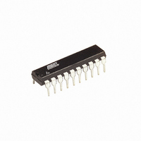
ATTINY2313-20PU Atmel, ATTINY2313-20PU Datasheet - Page 112

ATTINY2313-20PU
Manufacturer Part Number
ATTINY2313-20PU
Description
IC MCU AVR 2K FLASH 20DIP
Manufacturer
Atmel
Series
AVR® ATtinyr
Datasheets
1.ATTINY2313-20MU.pdf
(226 pages)
2.ATTINY2313V-10MU.pdf
(15 pages)
3.ATTINY2313V-10SU.pdf
(20 pages)
Specifications of ATTINY2313-20PU
Core Processor
AVR
Core Size
8-Bit
Speed
20MHz
Connectivity
SPI, UART/USART
Peripherals
Brown-out Detect/Reset, POR, PWM, WDT
Number Of I /o
18
Program Memory Size
2KB (1K x 16)
Program Memory Type
FLASH
Eeprom Size
128 x 8
Ram Size
128 x 8
Voltage - Supply (vcc/vdd)
2.7 V ~ 5.5 V
Oscillator Type
Internal
Operating Temperature
-40°C ~ 85°C
Package / Case
20-DIP (0.300", 7.62mm)
Package
20PDIP
Device Core
AVR
Family Name
ATtiny
Maximum Speed
20 MHz
Operating Supply Voltage
3.3|5 V
Data Bus Width
8 Bit
Number Of Programmable I/os
18
Interface Type
SPI/USART/USI
Number Of Timers
2
Processor Series
ATTINY2x
Core
AVR8
Data Ram Size
128 B
Maximum Clock Frequency
20 MHz
Maximum Operating Temperature
+ 85 C
Mounting Style
Through Hole
3rd Party Development Tools
EWAVR, EWAVR-BL
Development Tools By Supplier
ATAVRDRAGON, ATSTK500, ATSTK600, ATAVRISP2, ATAVRONEKIT
Minimum Operating Temperature
- 40 C
Cpu Family
ATtiny
Device Core Size
8b
Frequency (max)
20MHz
Total Internal Ram Size
128Byte
# I/os (max)
18
Number Of Timers - General Purpose
2
Operating Supply Voltage (typ)
3.3/5V
Operating Supply Voltage (max)
5.5V
Operating Supply Voltage (min)
2.7V
Instruction Set Architecture
RISC
Operating Temp Range
-40C to 85C
Operating Temperature Classification
Industrial
Mounting
Through Hole
Pin Count
20
Package Type
PDIP
For Use With
ATSTK600-DIP40 - STK600 SOCKET/ADAPTER 40-PDIP770-1007 - ISP 4PORT ATMEL AVR MCU SPI/JTAGATAVRDRAGON - KIT DRAGON 32KB FLASH MEM AVRATAVRISP2 - PROGRAMMER AVR IN SYSTEMATJTAGICE2 - AVR ON-CHIP D-BUG SYSTEM
Lead Free Status / RoHS Status
Lead free / RoHS Compliant
Data Converters
-
Lead Free Status / Rohs Status
Lead free / RoHS Compliant
Available stocks
Company
Part Number
Manufacturer
Quantity
Price
Part Number:
ATTINY2313-20PU
Manufacturer:
ATMEL/爱特梅尔
Quantity:
20 000
AVR USART vs. AVR
UART – Compatibility
Clock Generation
112
ATtiny2313
The dashed boxes in the block diagram separate the three main parts of the USART (listed from
the top): Clock Generator, Transmitter and Receiver. Control registers are shared by all units.
The Clock Generation logic consists of synchronization logic for external clock input used by
synchronous slave operation, and the baud rate generator. The XCK (Transfer Clock) pin is only
used by synchronous transfer mode. The Transmitter consists of a single write buffer, a serial
Shift Register, Parity Generator and Control logic for handling different serial frame formats. The
write buffer allows a continuous transfer of data without any delay between frames. The
Receiver is the most complex part of the USART module due to its clock and data recovery
units. The recovery units are used for asynchronous data reception. In addition to the recovery
units, the Receiver includes a Parity Checker, Control logic, a Shift Register and a two level
receive buffer (UDR). The Receiver supports the same frame formats as the Transmitter, and
can detect Frame Error, Data OverRun and Parity Errors.
The USART is fully compatible with the AVR UART regarding:
•
•
•
•
•
However, the receive buffering has two improvements that will affect the compatibility in some
special cases:
•
•
The following control bits have changed name, but have same functionality and register location:
•
•
The Clock Generation logic generates the base clock for the Transmitter and Receiver. The
USART supports four modes of clock operation: Normal asynchronous, Double Speed asyn-
chronous, Master synchronous and Slave synchronous mode. The UMSEL bit in USART
Control and Status Register C (UCSRC) selects between asynchronous and synchronous oper-
ation. Double Speed (asynchronous mode only) is controlled by the U2X found in the UCSRA
Register. When using synchronous mode (UMSEL = 1), the Data Direction Register for the XCK
pin (DDR_XCK) controls whether the clock source is internal (Master mode) or external (Slave
mode). The XCK pin is only active when using synchronous mode.
Figure 54
Bit locations inside all USART Registers.
Baud Rate Generation.
Transmitter Operation.
Transmit Buffer Functionality.
Receiver Operation.
A second Buffer Register has been added. The two Buffer Registers operate as a circular
FIFO buffer. Therefore the UDR must only be read once for each incoming data! More
important is the fact that the error flags (FE and DOR) and the ninth data bit (RXB8) are
buffered with the data in the receive buffer. Therefore the status bits must always be read
before the UDR Register is read. Otherwise the error status will be lost since the buffer state
is lost.
The Receiver Shift Register can now act as a third buffer level. This is done by allowing the
received data to remain in the serial Shift Register (see
full, until a new start bit is detected. The USART is therefore more resistant to Data OverRun
(DOR) error conditions.
CHR9 is changed to UCSZ2.
OR is changed to DOR.
shows a block diagram of the clock generation logic.
Figure
53) if the Buffer Registers are
2543L–AVR–08/10


