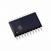
PIC24F16KA101-I/SO Microchip Technology, PIC24F16KA101-I/SO Datasheet - Page 176

PIC24F16KA101-I/SO
Manufacturer Part Number
PIC24F16KA101-I/SO
Description
IC PIC MCU FLASH 16K 20-SOIC
Manufacturer
Microchip Technology
Series
PIC® XLP™ 24Fr
Datasheets
1.MA240017.pdf
(254 pages)
2.PIC24F04KA201-ISS.pdf
(48 pages)
3.PIC24F16KA101-ISS.pdf
(18 pages)
Specifications of PIC24F16KA101-I/SO
Program Memory Type
FLASH
Program Memory Size
16KB (5.5K x 24)
Package / Case
20-SOIC (7.5mm Width)
Core Processor
PIC
Core Size
16-Bit
Speed
32MHz
Connectivity
I²C, IrDA, SPI, UART/USART
Peripherals
Brown-out Detect/Reset, POR, PWM, WDT
Number Of I /o
18
Eeprom Size
512 x 8
Ram Size
1.5K x 8
Voltage - Supply (vcc/vdd)
1.8 V ~ 3.6 V
Data Converters
A/D 9x10b
Oscillator Type
Internal
Operating Temperature
-40°C ~ 85°C
Processor Series
PIC24F
Core
PIC
Data Bus Width
16 bit
Data Ram Size
1.5 KB
Interface Type
I2C/IrDA/SPI/UART
Maximum Clock Frequency
32 MHz
Number Of Programmable I/os
18
Number Of Timers
3
Operating Supply Voltage
1.8 V to 3.6 V
Maximum Operating Temperature
+ 85 C
Mounting Style
SMD/SMT
3rd Party Development Tools
52713-733, 52714-737, 53276-922, EWDSPIC
Development Tools By Supplier
PG164130, DV164035, DV244005, DV164005, DM240001
Minimum Operating Temperature
- 40 C
On-chip Adc
9-ch x 10-bit
Lead Free Status / RoHS Status
Lead free / RoHS Compliant
For Use With
MA240017 - MODULE PLUG-IN PIC24F16KA102 PIM
Lead Free Status / Rohs Status
Lead free / RoHS Compliant
- Current page: 176 of 254
- Download datasheet (4Mb)
PIC24F16KA102 FAMILY
-
REGISTER 22-4:
DS39927B-page 174
bit 15
bit 7
Legend:
R = Readable bit
-n = Value at POR
bit 15
bit 14-12
bit 11-8
bit 7
bit 6-5
bit 4-0
CH0NB
CH0NA
R/W-0
R/W-0
CH0NB: Channel 0 Negative Input Select for MUX B Multiplexer Setting bit
1 = Channel 0 negative input is AN1
0 = Channel 0 negative input is V
Unimplemented: Read as ‘0’
CH0SB<3:0>: Channel 0 Positive Input Select for MUX B Multiplexer Setting bits
1111 = Channel 0 positive input is band gap reference (V
1110 = Channel 0 positive input is band gap, divided by two, reference (V
1101 = No channels connected (actual ADC MUX switch activates but input floats); used for CTMU
1100 = Channel 0 positive input is AN12
1011 = Channel 0 positive input is AN11
1010 = Channel 0 positive input is AN10
1001 = Reserved
1000 = Reserved
0110 = AV
0110 = AV
0101 = Channel 0 positive input is AN5
0100 = Channel 0 positive input is AN4
0010 = Channel 0 positive input is AN3
0010 = Channel 0 positive input is AN2
0001 = Channel 0 positive input is AN1
0000 = Channel 0 positive input is AN0
CH0NA: Channel 0 Negative Input Select for MUX A Multiplexer Setting bit
1 = Channel 0 negative input is AN1
0 = Channel 0 negative input is V
Unimplemented: Read as ‘0’
CH0SA<4:0>: Channel 0 Positive Input Select for Sample A bits
1111 = Channel 0 positive input is band gap reference (V
1110 = Channel 0 positive input is band gap, divided by two, reference (V
1101 = No channels connected (actual ADC MUX switch activates but input floats); used for CTMU
1100 = Channel 0 positive input is AN12
1011 = Channel 0 positive input is AN11
1010 = Channel 0 positive input is AN10
1001 = Reserved
1000 = Reserved
0110 = AV
0110 = AV
0101 = Channel 0 positive input is AN5
0100 = Channel 0 positive input is AN4
0010 = Channel 0 positive input is AN3
0010 = Channel 0 positive input is AN2
0001 = Channel 0 positive input is AN1
0000 = Channel 0 positive input is AN0
U-0
U-0
—
—
AD1CHS: A/D INPUT SELECT REGISTER
DD
SS
DD
SS
W = Writable bit
‘1’ = Bit is set
U-0
U-0
—
—
CH0SA4
R/W-0
R
R
U-0
-
-
—
Preliminary
U = Unimplemented bit, read as ‘0’
‘0’ = Bit is cleared
CH0SB3
CH0SA3
R/W-0
R/W-0
BG
BG
)
)
CH0SB2
CH0SA2
R/W-0
R/W-0
© 2009 Microchip Technology Inc.
x = Bit is unknown
BG
BG
CH0SB1
CH0SA1
/2)
/2)
R/W-0
R/W-0
CH0SB0
CH0SA0
R/W-0
R/W-0
bit 8
bit 0
Related parts for PIC24F16KA101-I/SO
Image
Part Number
Description
Manufacturer
Datasheet
Request
R

Part Number:
Description:
Manufacturer:
Microchip Technology Inc.
Datasheet:

Part Number:
Description:
Manufacturer:
Microchip Technology Inc.
Datasheet:

Part Number:
Description:
Manufacturer:
Microchip Technology Inc.
Datasheet:

Part Number:
Description:
Manufacturer:
Microchip Technology Inc.
Datasheet:

Part Number:
Description:
Manufacturer:
Microchip Technology Inc.
Datasheet:

Part Number:
Description:
Manufacturer:
Microchip Technology Inc.
Datasheet:

Part Number:
Description:
Manufacturer:
Microchip Technology Inc.
Datasheet:

Part Number:
Description:
Manufacturer:
Microchip Technology Inc.
Datasheet:


