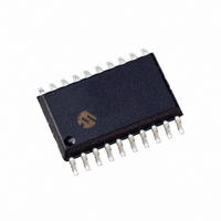
PIC24F16KA101-I/SO Microchip Technology, PIC24F16KA101-I/SO Datasheet - Page 181

PIC24F16KA101-I/SO
Manufacturer Part Number
PIC24F16KA101-I/SO
Description
IC PIC MCU FLASH 16K 20-SOIC
Manufacturer
Microchip Technology
Series
PIC® XLP™ 24Fr
Datasheets
1.MA240017.pdf
(254 pages)
2.PIC24F04KA201-ISS.pdf
(48 pages)
3.PIC24F16KA101-ISS.pdf
(18 pages)
Specifications of PIC24F16KA101-I/SO
Program Memory Type
FLASH
Program Memory Size
16KB (5.5K x 24)
Package / Case
20-SOIC (7.5mm Width)
Core Processor
PIC
Core Size
16-Bit
Speed
32MHz
Connectivity
I²C, IrDA, SPI, UART/USART
Peripherals
Brown-out Detect/Reset, POR, PWM, WDT
Number Of I /o
18
Eeprom Size
512 x 8
Ram Size
1.5K x 8
Voltage - Supply (vcc/vdd)
1.8 V ~ 3.6 V
Data Converters
A/D 9x10b
Oscillator Type
Internal
Operating Temperature
-40°C ~ 85°C
Processor Series
PIC24F
Core
PIC
Data Bus Width
16 bit
Data Ram Size
1.5 KB
Interface Type
I2C/IrDA/SPI/UART
Maximum Clock Frequency
32 MHz
Number Of Programmable I/os
18
Number Of Timers
3
Operating Supply Voltage
1.8 V to 3.6 V
Maximum Operating Temperature
+ 85 C
Mounting Style
SMD/SMT
3rd Party Development Tools
52713-733, 52714-737, 53276-922, EWDSPIC
Development Tools By Supplier
PG164130, DV164035, DV244005, DV164005, DM240001
Minimum Operating Temperature
- 40 C
On-chip Adc
9-ch x 10-bit
Lead Free Status / RoHS Status
Lead free / RoHS Compliant
For Use With
MA240017 - MODULE PLUG-IN PIC24F16KA102 PIM
Lead Free Status / Rohs Status
Lead free / RoHS Compliant
- Current page: 181 of 254
- Download datasheet (4Mb)
23.0
The comparator module provides two dual input
comparators. The inputs to the comparator can be
configured to use any one of four external analog
inputs, as well as a voltage reference input from either
the internal band gap reference divided by 2 (V
the comparator voltage reference generator.
FIGURE 23-1:
© 2009 Microchip Technology Inc.
Note:
CCH<1:0>
CREF
C
C
C
V
C
CV
X
X
X
BG
X
COMPARATOR MODULE
INB
INC
IND
INA
REF
/2
This data sheet summarizes the features
of this group of PIC24F devices. It is not
intended to be a comprehensive reference
source. For more information on the
Comparator module, refer to the “PIC24F
Family Reference Manual”, Section 19.
“Comparator Module” (DS39710).
COMPARATOR MODULE BLOCK DIAGRAM
Select
Logic
Input
V
V
V
V
IN
IN
IN
IN
-
+
-
+
C1
C2
BG
/2) or
Preliminary
PIC24F16KA102 FAMILY
EVPOL<1:0>
EVPOL<1:0>
CPOL
CPOL
The comparator outputs may be directly connected to
the CxOUT pins. When the respective COE equals ‘1’,
the I/O pad logic makes the unsynchronized output of
the comparator available on the pin.
A simplified block diagram of the module is displayed in
Figure 23-1. Diagrams of the possible individual
comparator
Figure 23-2.
Each comparator has its own control register,
CMxCON (Register 23-1), for enabling and configuring
its operation. The output and event status of all three
comparators is provided in the CMSTAT register
(Register 23-2).
Trigger/Interrupt
Trigger/Interrupt
Logic
Logic
configurations
COE
COE
CEVT
CEVT
COUT
COUT
are
DS39927B-page 179
C1OUT
C2OUT
displayed
Pin
Pin
in
Related parts for PIC24F16KA101-I/SO
Image
Part Number
Description
Manufacturer
Datasheet
Request
R

Part Number:
Description:
Manufacturer:
Microchip Technology Inc.
Datasheet:

Part Number:
Description:
Manufacturer:
Microchip Technology Inc.
Datasheet:

Part Number:
Description:
Manufacturer:
Microchip Technology Inc.
Datasheet:

Part Number:
Description:
Manufacturer:
Microchip Technology Inc.
Datasheet:

Part Number:
Description:
Manufacturer:
Microchip Technology Inc.
Datasheet:

Part Number:
Description:
Manufacturer:
Microchip Technology Inc.
Datasheet:

Part Number:
Description:
Manufacturer:
Microchip Technology Inc.
Datasheet:

Part Number:
Description:
Manufacturer:
Microchip Technology Inc.
Datasheet:


