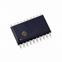
DSPIC33FJ12MC201-I/SO Microchip Technology, DSPIC33FJ12MC201-I/SO Datasheet - Page 10

DSPIC33FJ12MC201-I/SO
Manufacturer Part Number
DSPIC33FJ12MC201-I/SO
Description
IC DSPIC MCU/DSP 12K 20SOIC
Manufacturer
Microchip Technology
Series
dsPIC™ 33Fr
Datasheets
1.PIC24HJ12GP201-ISO.pdf
(84 pages)
2.DSPIC33FJ12MC201-ISO.pdf
(288 pages)
3.DSPIC33FJ12MC201-ISO.pdf
(14 pages)
4.DSPIC33FJ12MC201-IP.pdf
(284 pages)
Specifications of DSPIC33FJ12MC201-I/SO
Program Memory Type
FLASH
Program Memory Size
12KB (12K x 8)
Package / Case
20-SOIC (7.5mm Width)
Core Processor
dsPIC
Core Size
16-Bit
Speed
40 MIPs
Connectivity
I²C, IrDA, SPI, UART/USART
Peripherals
Brown-out Detect/Reset, Motor Control PWM, QEI, POR, PWM, WDT
Number Of I /o
15
Ram Size
1K x 8
Voltage - Supply (vcc/vdd)
3 V ~ 3.6 V
Data Converters
A/D 4x10b
Oscillator Type
Internal
Operating Temperature
-40°C ~ 85°C
Product
DSCs
Data Bus Width
16 bit
Processor Series
DSPIC33F
Core
dsPIC
Maximum Clock Frequency
40 MHz
Number Of Programmable I/os
15
Data Ram Size
1 KB
Maximum Operating Temperature
+ 85 C
Mounting Style
SMD/SMT
3rd Party Development Tools
52713-733, 52714-737, 53276-922, EWDSPIC
Development Tools By Supplier
PG164130, DV164035, DV244005, DV164005, PG164120, DM240001, DV164033
Minimum Operating Temperature
- 40 C
Lead Free Status / RoHS Status
Lead free / RoHS Compliant
For Use With
DV164033 - KIT START EXPLORER 16 MPLAB ICD2DM240001 - BOARD DEMO PIC24/DSPIC33/PIC32
Eeprom Size
-
Lead Free Status / Rohs Status
Lead free / RoHS Compliant
FIGURE 3-3:
3.4
The term “Blank Check” implies verifying that the
device has been successfully erased and has no
programmed memory locations. A blank or erased
memory location is always read as ‘1’.
The Device ID registers (0xFF0000:0xFF0002) can be
ignored by the Blank Check since this region stores
device information that cannot be erased. The device
Configuration registers are also ignored by the Blank
Check. Additionally, all unimplemented memory space
should be ignored from the Blank Check.
The QBLANK command is used for the Blank Check. It
determines if the code memory is erased by testing
these memory regions. A ‘BLANK’ or ‘NOT BLANK’
response is returned. If it is determined that the device
is not blank, it must be erased before attempting to
program the chip.
DS70152H-page 10
MCLR
V
PGDx
PGCx
DD
Blank Check
P6
ENTERING ENHANCED ICSP™ MODE
P14
P18
V
b31
IH
0
b30
1
Program/Verify Entry Code = 0x4D434850
b29
0
b28
P1A
0
P1B
b27
1
3.5
3.5.1
Code memory is programmed with the PROGP
command. PROGP programs one row of code memory
starting from the memory address specified in the
command. The number of PROGP commands required
to program a device depends on the number of write
blocks that must be programmed in the device.
A flowchart for programming code memory is illustrated
in
of a dsPIC33F/PIC24H device are programmed. First,
the
‘RemainingCmds’ in the flowchart) is set to 1368 and
the destination address (called ‘BaseAddress’) is set to
‘0’. Next, one write block in the device is programmed
with a PROGP command. Each PROGP command
contains data for one row of code memory of the
dsPIC33F/PIC24H.
processed
decremented by ‘1’ and compared with ‘0’. Since there
are more PROGP commands to send, ‘BaseAddress’ is
incremented by 0x80 to point to the next row of
memory.
On the second PROGP command, the second row is
programmed. This process is repeated until the entire
device is programmed.
Figure
Note:
...
number
Code Memory Programming
3-4. In this example, all 88K instruction words
b3
0
PROGRAMMING METHODOLOGY
If a bootloader needs to be programmed,
the
programmed into the first page of code
memory. For example, if a bootloader
located at address 0x200 attempts to
erase the first page, it would inadvertently
erase
bootloader into the second page (e.g.,
0x400).
successfully,
b2
of
0
bootloader
itself.
commands
After
b1
0
© 2010 Microchip Technology Inc.
V
IH
b0
0
Instead,
the
code
‘RemainingCmds’
P19
first
to
must
program
send
command
P7
not
(called
the
be
is
is


