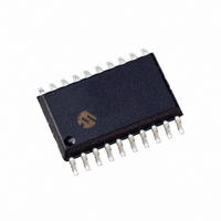
DSPIC33FJ12MC201-I/SO Microchip Technology, DSPIC33FJ12MC201-I/SO Datasheet - Page 11

DSPIC33FJ12MC201-I/SO
Manufacturer Part Number
DSPIC33FJ12MC201-I/SO
Description
IC DSPIC MCU/DSP 12K 20SOIC
Manufacturer
Microchip Technology
Series
dsPIC™ 33Fr
Datasheets
1.PIC24HJ12GP201-ISO.pdf
(84 pages)
2.DSPIC33FJ12MC201-ISO.pdf
(288 pages)
3.DSPIC33FJ12MC201-ISO.pdf
(14 pages)
4.DSPIC33FJ12MC201-IP.pdf
(284 pages)
Specifications of DSPIC33FJ12MC201-I/SO
Program Memory Type
FLASH
Program Memory Size
12KB (12K x 8)
Package / Case
20-SOIC (7.5mm Width)
Core Processor
dsPIC
Core Size
16-Bit
Speed
40 MIPs
Connectivity
I²C, IrDA, SPI, UART/USART
Peripherals
Brown-out Detect/Reset, Motor Control PWM, QEI, POR, PWM, WDT
Number Of I /o
15
Ram Size
1K x 8
Voltage - Supply (vcc/vdd)
3 V ~ 3.6 V
Data Converters
A/D 4x10b
Oscillator Type
Internal
Operating Temperature
-40°C ~ 85°C
Product
DSCs
Data Bus Width
16 bit
Processor Series
DSPIC33F
Core
dsPIC
Maximum Clock Frequency
40 MHz
Number Of Programmable I/os
15
Data Ram Size
1 KB
Maximum Operating Temperature
+ 85 C
Mounting Style
SMD/SMT
3rd Party Development Tools
52713-733, 52714-737, 53276-922, EWDSPIC
Development Tools By Supplier
PG164130, DV164035, DV244005, DV164005, PG164120, DM240001, DV164033
Minimum Operating Temperature
- 40 C
Lead Free Status / RoHS Status
Lead free / RoHS Compliant
For Use With
DV164033 - KIT START EXPLORER 16 MPLAB ICD2DM240001 - BOARD DEMO PIC24/DSPIC33/PIC32
Eeprom Size
-
Lead Free Status / Rohs Status
Lead free / RoHS Compliant
FIGURE 3-4:
© 2010 Microchip Technology Inc.
BaseAddress + 0x80
BaseAddress =
No
RemainingCmds = 1368
RemainingCmds =
RemainingCmds – 1
BaseAddress = 0x0
Command to Program
FLOWCHART FOR
PROGRAMMING CODE
MEMORY
RemainingCmds
BaseAddress
PROGP response
Send PROGP
PASS?
Start
‘0’?
End
Is
Is
Yes
Yes
Report Error
No
Failure
3.5.2
After code memory is programmed, the contents of
memory can be verified to ensure that programming
was successful. Verification requires code memory to
be read back and compared against the copy held in
the programmer’s buffer.
The READP command can be used to read back all the
programmed code memory.
Alternatively, you can have the programmer perform
the verification after the entire device is programmed,
using a checksum computation.
3.5.3
Only the Configuration registers are included in the
checksum computation. The Device ID and Unit ID are
not included in the checksum computation.
TABLE D-1: “CHECKSUM COMPUTATION”
how this 16-bit computation can be made for each
dsPIC33F and PIC24H device. Computations for read
code protection are shown both enabled and disabled.
The checksum values shown here assume that the
Configuration registers are also erased. However,
when code protection is enabled, the value of the FGS
register is assumed to be 0x5.
PROGRAMMING VERIFICATION
CHECKSUM COMPUTATION
DS70152H-page 11
shows


