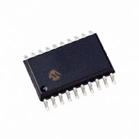
DSPIC33FJ12MC201-I/SO Microchip Technology, DSPIC33FJ12MC201-I/SO Datasheet - Page 19

DSPIC33FJ12MC201-I/SO
Manufacturer Part Number
DSPIC33FJ12MC201-I/SO
Description
IC DSPIC MCU/DSP 12K 20SOIC
Manufacturer
Microchip Technology
Series
dsPIC™ 33Fr
Datasheets
1.PIC24HJ12GP201-ISO.pdf
(84 pages)
2.DSPIC33FJ12MC201-ISO.pdf
(288 pages)
3.DSPIC33FJ12MC201-ISO.pdf
(14 pages)
4.DSPIC33FJ12MC201-IP.pdf
(284 pages)
Specifications of DSPIC33FJ12MC201-I/SO
Program Memory Type
FLASH
Program Memory Size
12KB (12K x 8)
Package / Case
20-SOIC (7.5mm Width)
Core Processor
dsPIC
Core Size
16-Bit
Speed
40 MIPs
Connectivity
I²C, IrDA, SPI, UART/USART
Peripherals
Brown-out Detect/Reset, Motor Control PWM, QEI, POR, PWM, WDT
Number Of I /o
15
Ram Size
1K x 8
Voltage - Supply (vcc/vdd)
3 V ~ 3.6 V
Data Converters
A/D 4x10b
Oscillator Type
Internal
Operating Temperature
-40°C ~ 85°C
Product
DSCs
Data Bus Width
16 bit
Processor Series
DSPIC33F
Core
dsPIC
Maximum Clock Frequency
40 MHz
Number Of Programmable I/os
15
Data Ram Size
1 KB
Maximum Operating Temperature
+ 85 C
Mounting Style
SMD/SMT
3rd Party Development Tools
52713-733, 52714-737, 53276-922, EWDSPIC
Development Tools By Supplier
PG164130, DV164035, DV244005, DV164005, PG164120, DM240001, DV164033
Minimum Operating Temperature
- 40 C
Lead Free Status / RoHS Status
Lead free / RoHS Compliant
For Use With
DV164033 - KIT START EXPLORER 16 MPLAB ICD2DM240001 - BOARD DEMO PIC24/DSPIC33/PIC32
Eeprom Size
-
Lead Free Status / Rohs Status
Lead free / RoHS Compliant
TABLE 3-9:
TABLE 3-10:
© 2010 Microchip Technology Inc.
0xF80000 FBS
0xF80002 FSS
0xF80004 FGS
0xF80006 FOSCSEL
0xF80008 FOSC
0xF8000A FWDT
0xF8000C FPOR
0xF8000E FICD
0xF80010 FUID0
0xF80012 FUID1
0xF80014 FUID2
0xF80016 FUID3
Legend: — = unimplemented bit, read as ‘0’.
Note 1:
0xF80000 FBS
0xF80004 FGS
0xF80006 FOSCSEL
0xF80008 FOSC
0xF8000A FWDT
0xF8000C FPOR
0xF8000E FICD
0xF80010 FCMP
Legend: — = unimplemented bit, read as ‘0’.
Note 1:
Address
Address
2:
3:
2:
3:
This Configuration register is not available and reads as 0xFF on dsPIC33FJ32MC302/304 devices.
These bits are reserved (read as ‘1’) and must be programmed as ‘1’.
The JTAGEN bit is set to ‘1’ by factory default. Microchip programmers such as MPLAB ICD 2 and REAL
ICE in-circuit emulator clear this bit by default when connecting to a device.
These bits are reserved (read as ‘1’) and must be programmed as ‘1’.
The JTAGEN bit is set to ‘1’ by factory default. Microchip programmers such as MPLAB ICD 2 and REAL
ICE in-circuit emulator clear this bit by default when connecting to a device.
These bits are reserved on dsPIC33FJXXXGS406 devices and always read as ‘1’.
Name
Name
(1)
dsPIC33FJ32MC302/304, dsPIC33FJ64MCX02/X04 AND dsPIC33FJ128MCX02/X04
DEVICE CONFIGURATION REGISTER MAP
dsPIC33FJ32GS406/606/608/610 AND dsPIC33FJ64GS406/606/608/610
DEVICE CONFIGURATION REGISTER MAP
FWDTEN
FWDTEN WINDIS
PWMPIN
IESO
Bit 7
IESO
Bit 7
FCKSM<1:0>
—
—
—
—
FCKSM<1:0>
Reserved
—
Reserved
RBS<1:0>
RSS<1:0>
WINDIS
ALTQIO
HPOL
(1)
Bit 6
Bit 6
(2)
—
—
—
—
—
—
CMMPOL1
JTAGEN
IOL1WAY
JTAGEN
ALTSS1
LPOL
Bit 5
Bit 5
—
—
—
—
—
—
—
—
—
—
(3)
(2)
(3)
User Unit ID Byte 0
User Unit ID Byte 1
User Unit ID Byte 2
User Unit ID Byte 3
WDTPRE
WDTPRE
ALTI2C
Bit 4
Bit 4
—
—
—
—
—
HYST1<1:0>
—
—
—
—
—
—
—
Bit 3
Bit 3
—
—
—
—
—
—
—
—
—
(3)
BSS<2:0>
SSS<2:0>
BSS<2:0>
OSCIOFNC POSCMD<1:0>
CMPPOL0
WDTPOST<3:0>
OSCIOFNC POSCMD<1:0>
WDTPOST<3:0>
Bit 2
Bit 2
—
GSS<1:0>
GSS<1:0>
—
FNOSC<2:0>
FPWRT<2:0>
FNOSC<2:0>
FPWRT<2:0>
(3)
DS70152H-page 19
Bit 1
HYST0<1:0>
Bit 1
ICS<1:0>
ICS<1:0>
GWRP
GWRP
BWRP
SWRP
BWRP
Bit 0
Bit 0
(3)


