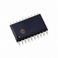
DSPIC33FJ12MC201-I/SO Microchip Technology, DSPIC33FJ12MC201-I/SO Datasheet - Page 32

DSPIC33FJ12MC201-I/SO
Manufacturer Part Number
DSPIC33FJ12MC201-I/SO
Description
IC DSPIC MCU/DSP 12K 20SOIC
Manufacturer
Microchip Technology
Series
dsPIC™ 33Fr
Datasheets
1.PIC24HJ12GP201-ISO.pdf
(84 pages)
2.DSPIC33FJ12MC201-ISO.pdf
(288 pages)
3.DSPIC33FJ12MC201-ISO.pdf
(14 pages)
4.DSPIC33FJ12MC201-IP.pdf
(284 pages)
Specifications of DSPIC33FJ12MC201-I/SO
Program Memory Type
FLASH
Program Memory Size
12KB (12K x 8)
Package / Case
20-SOIC (7.5mm Width)
Core Processor
dsPIC
Core Size
16-Bit
Speed
40 MIPs
Connectivity
I²C, IrDA, SPI, UART/USART
Peripherals
Brown-out Detect/Reset, Motor Control PWM, QEI, POR, PWM, WDT
Number Of I /o
15
Ram Size
1K x 8
Voltage - Supply (vcc/vdd)
3 V ~ 3.6 V
Data Converters
A/D 4x10b
Oscillator Type
Internal
Operating Temperature
-40°C ~ 85°C
Product
DSCs
Data Bus Width
16 bit
Processor Series
DSPIC33F
Core
dsPIC
Maximum Clock Frequency
40 MHz
Number Of Programmable I/os
15
Data Ram Size
1 KB
Maximum Operating Temperature
+ 85 C
Mounting Style
SMD/SMT
3rd Party Development Tools
52713-733, 52714-737, 53276-922, EWDSPIC
Development Tools By Supplier
PG164130, DV164035, DV244005, DV164005, PG164120, DM240001, DV164033
Minimum Operating Temperature
- 40 C
Lead Free Status / RoHS Status
Lead free / RoHS Compliant
For Use With
DV164033 - KIT START EXPLORER 16 MPLAB ICD2DM240001 - BOARD DEMO PIC24/DSPIC33/PIC32
Eeprom Size
-
Lead Free Status / Rohs Status
Lead free / RoHS Compliant
5.0
ICSP mode is a special programming protocol that
allows you to read and write to dsPIC33F/PIC24H
device family memory. The ICSP mode is the most
direct method used to program the device; however,
note that Enhanced ICSP is faster. ICSP mode also
has the ability to read the contents of executive
memory to determine if the programming executive is
present. This capability is accomplished by applying
control codes and instructions serially to the device
using pins PGCx and PGDx.
In ICSP mode, the system clock is taken from the
PGCx pin, regardless of the device’s oscillator Config-
uration bits. All instructions are shifted serially into an
internal buffer, then loaded into the instruction register
and executed. No program fetching occurs from inter-
nal memory. Instructions are fed in 24 bits at a time.
PGDx is used to shift data in, and PGCx is used as both
the serial shift clock and the CPU execution clock.
DS70152H-page 32
Note:
Note:
DEVICE PROGRAMMING – ICSP
Any development tool that modifies the con-
figuration memory on dsPIC33FJ06GS101/
102/202,
504, dsPIC33FJ32GS406/606/608/610 and
dsPIC33FJ64GS406/606/608/610 devices
must take care to preserve the data con-
tained in the last six words of program mem-
ory. Refer to
Calibration
information.
During ICSP operation, the operating
frequency of PGCx must not exceed
5 MHz.
Appendix C: “Diagnostic and
dsPIC33FJ16GS402/404/502/
Registers”
for
more
5.1
Figure 5-1
programming process. After entering ICSP mode, the
first action is to Bulk Erase the device. Next, the code
memory is programmed, followed by the device
Configuration registers. Code memory (including the
Configuration registers) is then verified to ensure that
programming was successful. Then, program the
code-protect Configuration bits, if required.
FIGURE 5-1:
Overview of the Programming
Process
illustrates the high-level overview of the
Program Configuration Bits
Verify Configuration Bits
Program Memory
Verify Program
Enter ICSP™
Perform Bulk
Exit ICSP
HIGH-LEVEL ICSP™
PROGRAMMING FLOW
© 2010 Microchip Technology Inc.
Erase
Start
End


