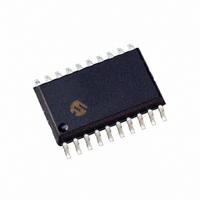
DSPIC33FJ12MC201-I/SO Microchip Technology, DSPIC33FJ12MC201-I/SO Datasheet - Page 60

DSPIC33FJ12MC201-I/SO
Manufacturer Part Number
DSPIC33FJ12MC201-I/SO
Description
IC DSPIC MCU/DSP 12K 20SOIC
Manufacturer
Microchip Technology
Series
dsPIC™ 33Fr
Datasheets
1.PIC24HJ12GP201-ISO.pdf
(84 pages)
2.DSPIC33FJ12MC201-ISO.pdf
(288 pages)
3.DSPIC33FJ12MC201-ISO.pdf
(14 pages)
4.DSPIC33FJ12MC201-IP.pdf
(284 pages)
Specifications of DSPIC33FJ12MC201-I/SO
Program Memory Type
FLASH
Program Memory Size
12KB (12K x 8)
Package / Case
20-SOIC (7.5mm Width)
Core Processor
dsPIC
Core Size
16-Bit
Speed
40 MIPs
Connectivity
I²C, IrDA, SPI, UART/USART
Peripherals
Brown-out Detect/Reset, Motor Control PWM, QEI, POR, PWM, WDT
Number Of I /o
15
Ram Size
1K x 8
Voltage - Supply (vcc/vdd)
3 V ~ 3.6 V
Data Converters
A/D 4x10b
Oscillator Type
Internal
Operating Temperature
-40°C ~ 85°C
Product
DSCs
Data Bus Width
16 bit
Processor Series
DSPIC33F
Core
dsPIC
Maximum Clock Frequency
40 MHz
Number Of Programmable I/os
15
Data Ram Size
1 KB
Maximum Operating Temperature
+ 85 C
Mounting Style
SMD/SMT
3rd Party Development Tools
52713-733, 52714-737, 53276-922, EWDSPIC
Development Tools By Supplier
PG164130, DV164035, DV244005, DV164005, PG164120, DM240001, DV164033
Minimum Operating Temperature
- 40 C
Lead Free Status / RoHS Status
Lead free / RoHS Compliant
For Use With
DV164033 - KIT START EXPLORER 16 MPLAB ICD2DM240001 - BOARD DEMO PIC24/DSPIC33/PIC32
Eeprom Size
-
Lead Free Status / Rohs Status
Lead free / RoHS Compliant
TABLE 8-1:
DS70152H-page 60
Standard Operating Conditions
Operating Temperature: –40ºC-85ºC. Programming at 25ºC is recommended.
Param
P9b
P10
P11
P12
P13
P14
P15
P16
P17
P18
P19
P20
P21
No.
Note 1: V
T
T
T
T
T
T
T
T
T
T
T
T
T
Symbol
2: Time depends on the FRC accuracy and the value of the FRC Oscillator tuning register. Refer to
DLY
DLY
DLY
DLY
DLY
R
VALID
DLY
HLD
KEY
KEY
DLY
MCLRH
±0.3V of V
“Electrical Characteristics” section in the specific device data sheet.
5
6
7
8
9
10 Delay between Last PGCx ↓ and MCLR ↓
3
1
2
11 Maximum Wait Time for Configuration
DD
must also be supplied to the AV
Delay between PGDx ↓ by Programming
Executive to PGDx Released by
Programming Executive
PGCx Low Time After Programming
Bulk Erase Time
Page Erase Time
Row Programming Time
MCLR Rise Time to Enter ICSP mode
Data Out Valid from PGCx ↑
MCLR ↓ to V
Delay from First MCLR ↓ to First PGCx ↑
for Key Sequence on PGDx
Delay from Last PGCx ↓ for Key Sequence
on PGDx to Second MCLR ↑
Register Programming
MCLR High Time
AC/DC CHARACTERISTICS AND TIMING REQUIREMENTS (CONTINUED)
DD
and V
DD
Characteristic
SS
↓
, respectively.
DD
pins during programming. AV
19.5
1.28
Min
400
330
15
10
25
—
—
—
—
0
1
Max
100
500
1.0
23
25
—
—
—
—
—
—
—
—
DD
Units
and AV
ms
ms
ms
ms
μs
ns
μs
ns
ns
μs
ns
μs
s
© 2010 Microchip Technology Inc.
SS
should always be within
Conditions
See Note 2
See Note 2
See Note 2
—
—
—
—
—
—
—
—
—
—


