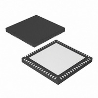
DSPIC33FJ128GP706A-I/MR Microchip Technology, DSPIC33FJ128GP706A-I/MR Datasheet - Page 35

DSPIC33FJ128GP706A-I/MR
Manufacturer Part Number
DSPIC33FJ128GP706A-I/MR
Description
IC DSPIC MCU/DSP 128K 64-QFN
Manufacturer
Microchip Technology
Series
dsPIC™ 33Fr
Datasheets
1.MCP3909T-ISS.pdf
(104 pages)
2.DSPIC33FJ12GP201-ISO.pdf
(90 pages)
3.DSPIC33FJ64GP206-IPT.pdf
(28 pages)
4.DSPIC33FJ64GP206A-IMR.pdf
(338 pages)
Specifications of DSPIC33FJ128GP706A-I/MR
Core Processor
dsPIC
Core Size
16-Bit
Speed
40 MIPs
Connectivity
CAN, I²C, IrDA, LIN, SPI, UART/USART
Peripherals
AC'97, Brown-out Detect/Reset, DMA, I²S, POR, PWM, WDT
Number Of I /o
53
Program Memory Size
128KB (128K x 8)
Program Memory Type
FLASH
Ram Size
16K x 8
Voltage - Supply (vcc/vdd)
3 V ~ 3.6 V
Data Converters
A/D 18x10b/12b
Oscillator Type
Internal
Operating Temperature
-40°C ~ 85°C
Package / Case
64-VFQFN, Exposed Pad
Product
DSCs
Processor Series
DSPIC33F
Core
dsPIC
3rd Party Development Tools
52713-733, 52714-737, 53276-922, EWDSPIC
Development Tools By Supplier
PG164130, DV164035, DV244005, DV164005, PG164120, DM240001, DV164033
Core Frequency
40MHz
Core Supply Voltage
3.3V
Embedded Interface Type
I2C, SPI, UART
No. Of I/o's
53
Flash Memory Size
128KB
Supply Voltage Range
3V To 3.6V
Rohs Compliant
No
Lead Free Status / RoHS Status
Lead free / RoHS Compliant
Eeprom Size
-
Lead Free Status / Rohs Status
Lead free / RoHS Compliant
3.5
© 2009 Microchip Technology Inc.
READING A/D DATA OF THE MCP3909 DEVICE
All three MCP3909 devices use the same clock source and reset signal, so all 6 A/D
channels of the 3 MCP3909 devices are synchronous. Only a single Data Ready (SDO)
signal of any of the MCP3909 device is required to read A/D data of the 3 phases in
turn. This module is invoked by IC1 interrupt triggered by the "data ready" signal on the
SDO of the MCP3909 device. IC1 is set to generate an interrupt for every two falling
edges. Therefore, only one of the two sampling data of the MCP3909 device is
read.The flow of reading the MCP3909 device's data is as follows:
• Retrieve all values of 3-phases, both current channel and voltage channel data.
• Accumulate the active power of each phase. On every other interrupt, the current
• Update the pointer of sampling array and length of sampling data. If the length of
FIGURE 3-5:
Bits 0-15 of each phase data are voltage channel data, bits 16-31 are current
channel data
and voltage values are stored into RAM in the cyclic sampling array
sampling data is 3-line cycles long, set the sampling complete flag, and then the
calculation function Calculate() will be called by the main flow to start computing
all corresponding parameters.
Flow Chart of Read A/D Data.
Select phase A of
The MCP3909 device,
clear SPI flag
Read MCP3909 data
Read phase A data
and accumulate active
energy of phase A
Read phase B data
and accumulate active
energy of phase B
Read phase C data
and accumulate active
energy of phase C
Even count
data read?
End
Yes
No
No
Update array pointer,
sample pass count
Read phase A data,
accumulate active
energy of phase A
and save data to array
Read phase A data,
accumulate active
energy of phase A
and save data to array
Read phase A data,
accumulate active
energy of phase A
and save data to array
flag and data length
Set data sampling
complete flag
End of sampling of
this cycle?
y
Firmware
DS51723A-page 35


