AT32UC3A0128-ALUT Atmel, AT32UC3A0128-ALUT Datasheet - Page 379
AT32UC3A0128-ALUT
Manufacturer Part Number
AT32UC3A0128-ALUT
Description
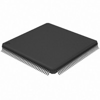
IC MCU AVR32 128KB FLASH 144LQFP
Manufacturer
Atmel
Series
AVR®32 UC3r
Specifications of AT32UC3A0128-ALUT
Core Processor
AVR
Core Size
32-Bit
Speed
66MHz
Connectivity
EBI/EMI, Ethernet, I²C, SPI, SSC, UART/USART, USB OTG
Peripherals
Brown-out Detect/Reset, POR, PWM, WDT
Number Of I /o
109
Program Memory Size
128KB (128K x 8)
Program Memory Type
FLASH
Ram Size
32K x 8
Voltage - Supply (vcc/vdd)
1.65 V ~ 1.95 V
Data Converters
A/D 8x10b
Oscillator Type
Internal
Operating Temperature
-40°C ~ 85°C
Package / Case
144-LQFP
Processor Series
AT32UC3x
Core
AVR32
Data Bus Width
32 bit
Data Ram Size
32 KB
Interface Type
2-Wire, RS-485, SPI, USART
Maximum Clock Frequency
66 MHz
Number Of Programmable I/os
69
Number Of Timers
3
Maximum Operating Temperature
+ 85 C
Mounting Style
SMD/SMT
3rd Party Development Tools
EWAVR32, EWAVR32-BL, KSK-EVK1100-PL
Development Tools By Supplier
ATAVRDRAGON, ATSTK500, ATSTK600, ATAVRISP2, ATAVRONEKIT, ATEXTWIFI, ATEVK1100, ATEVK1105
Minimum Operating Temperature
- 40 C
Controller Family/series
AT32UC3A
No. Of I/o's
109
Ram Memory Size
32KB
Cpu Speed
66MHz
No. Of Timers
1
Rohs Compliant
Yes
For Use With
ATEVK1105 - KIT EVAL FOR AT32UC3A0ATAVRONEKIT - KIT AVR/AVR32 DEBUGGER/PROGRMMR770-1008 - ISP 4PORT ATMEL AVR32 MCU SPIATEVK1100 - KIT DEV/EVAL FOR AVR32 AT32UC3A
Lead Free Status / RoHS Status
Lead free / RoHS Compliant
Eeprom Size
-
Lead Free Status / Rohs Status
Lead free / RoHS Compliant
Available stocks
Company
Part Number
Manufacturer
Quantity
Price
Company:

Part Number:
AT32UC3A0128-ALUT
Manufacturer:
Atmel
Quantity:
166


32058J–AVR32–04/11
– Write Cycle
– Null Delay Setup and Hold
Figure 27-13. Write Cycle
The write_cycle time is defined as the total duration of the write cycle, that is, from the time
where address is set on the address bus to the point where address may change. The total write
cycle time is equal to:
NWE_CYCLE = NWE_SETUP + NWE_PULSE + NWE_HOLD
= NCS_WR_SETUP + NCS_WR_PULSE + NCS_WR_HOLD
All NWE and NCS (write) timings are defined separately for each chip select as an integer num-
ber of Master Clock cycles. To ensure that the NWE and NCS timings are coherent, the user
must define the total write cycle instead of the hold timing. This implicitly defines the NWE hold
time and NCS (write) hold times as:
NWE_HOLD = NWE_CYCLE - NWE_SETUP - NWE_PULSE
NCS_WR_HOLD = NWE_CYCLE - NCS_WR_SETUP - NCS_WR_PULSE
If null setup parameters are programmed for NWE and/or NCS, NWE and/or NCS remain active
continuously in case of consecutive write cycles in the same memory (see
ever, for devices that perform write operations on the rising edge of NWE or NCS, such as
SRAM, either a setup or a hold must be programmed.
NBS0, NBS1,
A0, A1
CLK_SMC
A[25:2]
NWE
NCS
NCS_WR_SETUP
NWE_SETUP
NCS_WR_PULSE
NWE_CYCLE
NWE_PULSE
NWE_HOLD
NCS_WR_HOLD
AT32UC3A
Figure
27-14). How-
379
Related parts for AT32UC3A0128-ALUT
Image
Part Number
Description
Manufacturer
Datasheet
Request
R

Part Number:
Description:
DEV KIT FOR AVR/AVR32
Manufacturer:
Atmel
Datasheet:

Part Number:
Description:
INTERVAL AND WIPE/WASH WIPER CONTROL IC WITH DELAY
Manufacturer:
ATMEL Corporation
Datasheet:
Part Number:
Description:
Low-Voltage Voice-Switched IC for Hands-Free Operation
Manufacturer:
ATMEL Corporation
Datasheet:
Part Number:
Description:
MONOLITHIC INTEGRATED FEATUREPHONE CIRCUIT
Manufacturer:
ATMEL Corporation
Datasheet:
Part Number:
Description:
AM-FM Receiver IC U4255BM-M
Manufacturer:
ATMEL Corporation
Datasheet:
Part Number:
Description:
Monolithic Integrated Feature Phone Circuit
Manufacturer:
ATMEL Corporation
Datasheet:
Part Number:
Description:
Multistandard Video-IF and Quasi Parallel Sound Processing
Manufacturer:
ATMEL Corporation
Datasheet:
Part Number:
Description:
High-performance EE PLD
Manufacturer:
ATMEL Corporation
Datasheet:
Part Number:
Description:
8-bit Flash Microcontroller
Manufacturer:
ATMEL Corporation
Datasheet:
Part Number:
Description:
2-Wire Serial EEPROM
Manufacturer:
ATMEL Corporation
Datasheet: