AT32UC3A0256-ALUT Atmel, AT32UC3A0256-ALUT Datasheet - Page 754
AT32UC3A0256-ALUT
Manufacturer Part Number
AT32UC3A0256-ALUT
Description
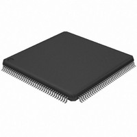
IC MCU AVR32 256KB FLASH 144LQFP
Manufacturer
Atmel
Series
AVR®32 UC3r
Specifications of AT32UC3A0256-ALUT
Core Processor
AVR
Core Size
32-Bit
Speed
66MHz
Connectivity
EBI/EMI, Ethernet, I²C, SPI, SSC, UART/USART, USB OTG
Peripherals
Brown-out Detect/Reset, POR, PWM, WDT
Number Of I /o
109
Program Memory Size
256KB (256K x 8)
Program Memory Type
FLASH
Ram Size
64K x 8
Voltage - Supply (vcc/vdd)
1.65 V ~ 1.95 V
Data Converters
A/D 8x10b
Oscillator Type
Internal
Operating Temperature
-40°C ~ 85°C
Package / Case
144-LQFP
Processor Series
AT32UC3x
Core
AVR32
Data Bus Width
32 bit
Data Ram Size
64 KB
Interface Type
2-Wire, RS-485, SPI, USART
Maximum Clock Frequency
66 MHz
Number Of Programmable I/os
69
Number Of Timers
3
Maximum Operating Temperature
+ 85 C
Mounting Style
SMD/SMT
3rd Party Development Tools
EWAVR32, EWAVR32-BL, KSK-EVK1100-PL
Development Tools By Supplier
ATAVRDRAGON, ATSTK500, ATSTK600, ATAVRISP2, ATAVRONEKIT, ATEXTWIFI, ATEVK1100, ATEVK1105
Minimum Operating Temperature
- 40 C
Controller Family/series
AT32UC3A
No. Of I/o's
109
Ram Memory Size
64KB
Cpu Speed
66MHz
No. Of Timers
1
Rohs Compliant
Yes
Package
144LQFP
Device Core
AVR32
Family Name
AT32
Maximum Speed
66 MHz
Operating Supply Voltage
1.8|3.3 V
For Use With
ATEVK1105 - KIT EVAL FOR AT32UC3A0ATAVRONEKIT - KIT AVR/AVR32 DEBUGGER/PROGRMMR770-1008 - ISP 4PORT ATMEL AVR32 MCU SPIATEVK1100 - KIT DEV/EVAL FOR AVR32 AT32UC3A
Lead Free Status / RoHS Status
Lead free / RoHS Compliant
Eeprom Size
-
Lead Free Status / Rohs Status
Lead free / RoHS Compliant
Available stocks
Company
Part Number
Manufacturer
Quantity
Price
Company:

Part Number:
AT32UC3A0256-ALUT
Manufacturer:
ATMEL
Quantity:
167


36.9.5
32058J–AVR32–04/11
MEMORY_WORD_ACCESS
Table 36-7.
Starting in Run-Test/Idle, SAB data are accessed in the following way:
For any operation, the full 36 bits of the address must be provided. For write operations, 32 data
bits must be provided, or the result will be undefined. For read operations, shifting may be termi-
nated once the required number of bits have been acquired.
Table 36-8.
This instruction allows access to the entire Service Access Bus data area. Data are accessed
through a 34-bit word index, a direction bit, and 32 bits of data. This instruction is identical to
MEMORY_SIZED_ACCESS except that it always does word sized accesses. The size field is
implied, and the two lowest address bits are removed.
Size field value
01
10
11
Instructions
IR input value
IR output value
DR Size
DR input value (Address phase)
DR input value (Data read phase)
DR input value (Data write phase)
DR output value (Address phase)
DR output value (Data read phase)
DR output value (Data write phase)
1. Select the DR Scan path.
2. Scan in the 36-bit address of the data to access, a 2-bit access size, and a direction bit
3. Go to Update-DR and re-enter Select-DR Scan.
4. For a read operation, scan out the contents of the addressed area. For a write opera-
5. Return to Run-Test/Idle.
(1=read, 0=write).
tion, scan in the new contents of the area.
Size Field Semantics
MEMORY_SIZED_ACCESS details
Access size
Halfword (16 bits)
Word (32 bits)
Reserved
Details
10101 (0x15)
peb01
39 bits
aaaaaaaa aaaaaaaa aaaaaaaa aaaaaaaa aaaassr
xxxxxxxx xxxxxxxx xxxxxxxx xxxxxxxx xxxxxxx
dddddddd dddddddd dddddddd dddddddd xxxxxxx
xxxxxxx xxxxxxxx xxxxxxxx xxxxxxxx xxxxxxeb
xxxxxeb dddddddd dddddddd dddddddd dddddddd
xxxxxxx xxxxxxxx xxxxxxxx xxxxxxxx xxxxxxeb
Data alignment
Address modulo 4 : data alignment
0: dddddddd dddddddd xxxxxxxx xxxxxxxx
1: Not allowed
2: xxxxxxxx xxxxxxxx dddddddd dddddddd
3: Not allowed
Address modulo 4 : data alignment
0: dddddddd dddddddd dddddddd dddddddd
1: Not allowed
2: Not allowed
3: Not allowed
N/A
AT32UC3A
754
Related parts for AT32UC3A0256-ALUT
Image
Part Number
Description
Manufacturer
Datasheet
Request
R

Part Number:
Description:
DEV KIT FOR AVR/AVR32
Manufacturer:
Atmel
Datasheet:

Part Number:
Description:
INTERVAL AND WIPE/WASH WIPER CONTROL IC WITH DELAY
Manufacturer:
ATMEL Corporation
Datasheet:
Part Number:
Description:
Low-Voltage Voice-Switched IC for Hands-Free Operation
Manufacturer:
ATMEL Corporation
Datasheet:
Part Number:
Description:
MONOLITHIC INTEGRATED FEATUREPHONE CIRCUIT
Manufacturer:
ATMEL Corporation
Datasheet:
Part Number:
Description:
AM-FM Receiver IC U4255BM-M
Manufacturer:
ATMEL Corporation
Datasheet:
Part Number:
Description:
Monolithic Integrated Feature Phone Circuit
Manufacturer:
ATMEL Corporation
Datasheet:
Part Number:
Description:
Multistandard Video-IF and Quasi Parallel Sound Processing
Manufacturer:
ATMEL Corporation
Datasheet:
Part Number:
Description:
High-performance EE PLD
Manufacturer:
ATMEL Corporation
Datasheet:
Part Number:
Description:
8-bit Flash Microcontroller
Manufacturer:
ATMEL Corporation
Datasheet:
Part Number:
Description:
2-Wire Serial EEPROM
Manufacturer:
ATMEL Corporation
Datasheet: