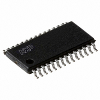
P89LPC932A1FDH,512 NXP Semiconductors, P89LPC932A1FDH,512 Datasheet - Page 2

P89LPC932A1FDH,512
Manufacturer Part Number
P89LPC932A1FDH,512
Description
IC 80C51 MCU FLASH 8K 28-TSSOP
Manufacturer
NXP Semiconductors
Series
LPC900r
Datasheet
1.P89LPC932A1FDH529.pdf
(64 pages)
Specifications of P89LPC932A1FDH,512
Program Memory Type
FLASH
Program Memory Size
8KB (8K x 8)
Package / Case
28-TSSOP
Core Processor
8051
Core Size
8-Bit
Speed
18MHz
Connectivity
I²C, SPI, UART/USART
Peripherals
Brown-out Detect/Reset, LED, POR, PWM, WDT
Number Of I /o
26
Ram Size
768 x 8
Voltage - Supply (vcc/vdd)
2.4 V ~ 3.6 V
Oscillator Type
Internal
Operating Temperature
-40°C ~ 85°C
Processor Series
P89LPC9x
Core
80C51
Data Bus Width
8 bit
Data Ram Size
768 B
Interface Type
I2C/SPI/UART
Maximum Clock Frequency
18 MHz
Number Of Programmable I/os
26
Number Of Timers
2
Operating Supply Voltage
2.4 V to 3.6 V
Maximum Operating Temperature
+ 85 C
Mounting Style
SMD/SMT
3rd Party Development Tools
PK51, CA51, A51, ULINK2
Minimum Operating Temperature
- 40 C
Cpu Family
89LP
Device Core
80C51
Device Core Size
8b
Frequency (max)
18MHz
Total Internal Ram Size
768Byte
# I/os (max)
26
Number Of Timers - General Purpose
2
Operating Supply Voltage (typ)
2.5/3.3V
Operating Supply Voltage (max)
3.6V
Operating Supply Voltage (min)
2.4V
Instruction Set Architecture
CISC
Operating Temp Range
-40C to 85C
Operating Temperature Classification
Industrial
Mounting
Surface Mount
Pin Count
28
Package Type
TSSOP
Lead Free Status / RoHS Status
Lead free / RoHS Compliant
For Use With
OM6292 - DEMO BOARD PCA2125 RTCDB-TSSOP-LPC932 - BOARD FOR LPC932 TSSOP622-1014 - BOARD FOR LPC9XX TSSOP622-1008 - BOARD FOR LPC9103 10-HVSON622-1006 - SOCKET ADAPTER BOARDMCB900K - BOARD PROTOTYPE NXP 89LPC9EPM900K - EMULATOR/PROGRAMMER NXP P89LPC9568-4000 - DEMO BOARD SPI/I2C TO DUAL UART568-3510 - DEMO BOARD SPI/I2C TO UART622-1003 - KIT FOR LCD DEMO622-1002 - USB IN-CIRCUIT PROG LPC9XX568-1759 - EMULATOR DEBUGGER/PROGRMMR LPC9X568-1758 - BOARD EVAL FOR LPC93X MCU FAMILY
Eeprom Size
-
Data Converters
-
Lead Free Status / Rohs Status
Lead free / RoHS Compliant
Other names
568-4515-5
935276132512
P89LPC932A1FDH
P89LPC932A1FDH
935276132512
P89LPC932A1FDH
P89LPC932A1FDH
NXP Semiconductors
P89LPC932A1_3
Product data sheet
2.3 Comparison to the P89LPC932
I
I
I
I
I
I
I
I
I
I
I
I
I
I
I
I
I
I
I
The P89LPC932A1 includes several improvements compared to the P89LPC932. Please
see P89LPC932A1 User manual for additional detailed information.
I
I
I
In-Circuit Programming (ICP) allows simple production coding with commercial
EPROM programmers. Flash security bits prevent reading of sensitive application
programs.
Serial flash In-System Programming (ISP) allows coding while the device is mounted
in the end application.
In-Application Programming (IAP) of the flash code memory. This allows changing the
code in a running application.
Watchdog timer with separate on-chip oscillator, requiring no external components.
The watchdog prescaler is selectable from eight values.
Low voltage reset (brownout detect) allows a graceful system shutdown when power
fails. May optionally be configured as an interrupt.
Idle and two different power-down reduced power modes. Improved wake-up from
Power-down mode (a LOW interrupt input starts execution). Typical power-down
current is 1 A (total power-down with voltage comparators disabled).
Active-LOW reset. On-chip power-on reset allows operation without external reset
components. A reset counter and reset glitch suppression circuitry prevent spurious
and incomplete resets. A software reset function is also available.
Configurable on-chip oscillator with frequency range options selected by user
programmed flash configuration bits. Oscillator options support frequencies from
20 kHz to the maximum operating frequency of 18 MHz.
Oscillator fail detect. The watchdog timer has a separate fully on-chip oscillator
allowing it to perform an oscillator fail detect function.
Programmable port output configuration options: quasi-bidirectional, open drain,
push-pull, input-only.
Port ‘input pattern match’ detect. Port 0 may generate an interrupt when the value of
the pins match or do not match a programmable pattern.
LED drive capability (20 mA) on all port pins. A maximum limit is specified for the
entire chip.
Controlled slew rate port outputs to reduce EMI. Outputs have approximately 10 ns
minimum ramp times.
Only power and ground connections are required to operate the P89LPC932A1 when
internal reset option is selected.
Four interrupt priority levels.
Eight keypad interrupt inputs, plus two additional external interrupt inputs.
Schmitt trigger port inputs.
Second data pointer.
Emulation support.
Byte-erasability has been added to the user code memory space.
All of the errata described in the P89LPC932 Errata sheet have been fixed.
Serial ICP has been added.
Rev. 03 — 12 March 2007
8-bit microcontroller with accelerated two-clock 80C51 core
P89LPC932A1
© NXP B.V. 2007. All rights reserved.
2 of 64


