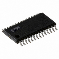
P89LPC932A1FDH,512 NXP Semiconductors, P89LPC932A1FDH,512 Datasheet - Page 20

P89LPC932A1FDH,512
Manufacturer Part Number
P89LPC932A1FDH,512
Description
IC 80C51 MCU FLASH 8K 28-TSSOP
Manufacturer
NXP Semiconductors
Series
LPC900r
Datasheet
1.P89LPC932A1FDH529.pdf
(64 pages)
Specifications of P89LPC932A1FDH,512
Program Memory Type
FLASH
Program Memory Size
8KB (8K x 8)
Package / Case
28-TSSOP
Core Processor
8051
Core Size
8-Bit
Speed
18MHz
Connectivity
I²C, SPI, UART/USART
Peripherals
Brown-out Detect/Reset, LED, POR, PWM, WDT
Number Of I /o
26
Ram Size
768 x 8
Voltage - Supply (vcc/vdd)
2.4 V ~ 3.6 V
Oscillator Type
Internal
Operating Temperature
-40°C ~ 85°C
Processor Series
P89LPC9x
Core
80C51
Data Bus Width
8 bit
Data Ram Size
768 B
Interface Type
I2C/SPI/UART
Maximum Clock Frequency
18 MHz
Number Of Programmable I/os
26
Number Of Timers
2
Operating Supply Voltage
2.4 V to 3.6 V
Maximum Operating Temperature
+ 85 C
Mounting Style
SMD/SMT
3rd Party Development Tools
PK51, CA51, A51, ULINK2
Minimum Operating Temperature
- 40 C
Cpu Family
89LP
Device Core
80C51
Device Core Size
8b
Frequency (max)
18MHz
Total Internal Ram Size
768Byte
# I/os (max)
26
Number Of Timers - General Purpose
2
Operating Supply Voltage (typ)
2.5/3.3V
Operating Supply Voltage (max)
3.6V
Operating Supply Voltage (min)
2.4V
Instruction Set Architecture
CISC
Operating Temp Range
-40C to 85C
Operating Temperature Classification
Industrial
Mounting
Surface Mount
Pin Count
28
Package Type
TSSOP
Lead Free Status / RoHS Status
Lead free / RoHS Compliant
For Use With
OM6292 - DEMO BOARD PCA2125 RTCDB-TSSOP-LPC932 - BOARD FOR LPC932 TSSOP622-1014 - BOARD FOR LPC9XX TSSOP622-1008 - BOARD FOR LPC9103 10-HVSON622-1006 - SOCKET ADAPTER BOARDMCB900K - BOARD PROTOTYPE NXP 89LPC9EPM900K - EMULATOR/PROGRAMMER NXP P89LPC9568-4000 - DEMO BOARD SPI/I2C TO DUAL UART568-3510 - DEMO BOARD SPI/I2C TO UART622-1003 - KIT FOR LCD DEMO622-1002 - USB IN-CIRCUIT PROG LPC9XX568-1759 - EMULATOR DEBUGGER/PROGRMMR LPC9X568-1758 - BOARD EVAL FOR LPC93X MCU FAMILY
Eeprom Size
-
Data Converters
-
Lead Free Status / Rohs Status
Lead free / RoHS Compliant
Other names
568-4515-5
935276132512
P89LPC932A1FDH
P89LPC932A1FDH
935276132512
P89LPC932A1FDH
P89LPC932A1FDH
NXP Semiconductors
P89LPC932A1_3
Product data sheet
7.12.1 External interrupt inputs
7.11 Data RAM arrangement
7.12 Interrupts
The P89LPC932A1 also has 512 bytes of on-chip Data EEPROM that is accessed via
SFRs (see
The 768 bytes of on-chip RAM are organized as shown in
Table 4.
The P89LPC932A1 uses a four priority level interrupt structure. This allows great flexibility
in controlling the handling of the many interrupt sources. The P89LPC932A1 supports
15 interrupt sources: external interrupts 0 and 1, timers 0 and 1, serial port Tx, serial port
Rx, combined serial port Rx/Tx, brownout detect, watchdog/RTC, I
comparators 1 and 2, SPI, CCU, and data EEPROM write completion.
Each interrupt source can be individually enabled or disabled by setting or clearing a bit in
the interrupt enable registers IEN0 or IEN1. The IEN0 register also contains a global
disable bit, EA, which disables all interrupts.
Each interrupt source can be individually programmed to one of four priority levels by
setting or clearing bits in the interrupt priority registers IP0, IP0H, IP1, and IP1H. An
interrupt service routine in progress can be interrupted by a higher priority interrupt, but
not by another interrupt of the same or lower priority. The highest priority interrupt service
cannot be interrupted by any other interrupt source. If two requests of different priority
levels are pending at the start of an instruction, the request of higher priority level is
serviced.
If requests of the same priority level are pending at the start of an instruction, an internal
polling sequence determines which request is serviced. This is called the arbitration
ranking. Note that the arbitration ranking is only used to resolve pending requests of the
same priority level.
The P89LPC932A1 has two external interrupt inputs as well as the Keypad Interrupt
function. The two interrupt inputs are identical to those present on the standard 80C51
microcontrollers.
These external interrupts can be programmed to be level-triggered or edge-triggered by
setting or clearing bit IT1 or IT0 in Register TCON.
Type
DATA
IDATA
XDATA
•
CODE
64 kB of Code memory space, accessed as part of program execution and via the
MOVC instruction. The P89LPC932A1 has 8 kB of on-chip Code memory.
On-chip data memory usages
Section 7.27 “Data
Data RAM
Memory that can be addressed directly and indirectly
Memory that can be addressed indirectly
Auxiliary (‘External Data’) on-chip memory that is accessed
using the MOVX instructions
Rev. 03 — 12 March 2007
8-bit microcontroller with accelerated two-clock 80C51 core
EEPROM”).
Table
P89LPC932A1
4.
2
C-bus, keyboard,
© NXP B.V. 2007. All rights reserved.
Size (bytes)
128
256
512
20 of 64


