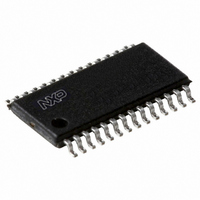
P89LPC932A1FDH,512 NXP Semiconductors, P89LPC932A1FDH,512 Datasheet - Page 43

P89LPC932A1FDH,512
Manufacturer Part Number
P89LPC932A1FDH,512
Description
IC 80C51 MCU FLASH 8K 28-TSSOP
Manufacturer
NXP Semiconductors
Series
LPC900r
Datasheet
1.P89LPC932A1FDH529.pdf
(64 pages)
Specifications of P89LPC932A1FDH,512
Program Memory Type
FLASH
Program Memory Size
8KB (8K x 8)
Package / Case
28-TSSOP
Core Processor
8051
Core Size
8-Bit
Speed
18MHz
Connectivity
I²C, SPI, UART/USART
Peripherals
Brown-out Detect/Reset, LED, POR, PWM, WDT
Number Of I /o
26
Ram Size
768 x 8
Voltage - Supply (vcc/vdd)
2.4 V ~ 3.6 V
Oscillator Type
Internal
Operating Temperature
-40°C ~ 85°C
Processor Series
P89LPC9x
Core
80C51
Data Bus Width
8 bit
Data Ram Size
768 B
Interface Type
I2C/SPI/UART
Maximum Clock Frequency
18 MHz
Number Of Programmable I/os
26
Number Of Timers
2
Operating Supply Voltage
2.4 V to 3.6 V
Maximum Operating Temperature
+ 85 C
Mounting Style
SMD/SMT
3rd Party Development Tools
PK51, CA51, A51, ULINK2
Minimum Operating Temperature
- 40 C
Cpu Family
89LP
Device Core
80C51
Device Core Size
8b
Frequency (max)
18MHz
Total Internal Ram Size
768Byte
# I/os (max)
26
Number Of Timers - General Purpose
2
Operating Supply Voltage (typ)
2.5/3.3V
Operating Supply Voltage (max)
3.6V
Operating Supply Voltage (min)
2.4V
Instruction Set Architecture
CISC
Operating Temp Range
-40C to 85C
Operating Temperature Classification
Industrial
Mounting
Surface Mount
Pin Count
28
Package Type
TSSOP
Lead Free Status / RoHS Status
Lead free / RoHS Compliant
For Use With
OM6292 - DEMO BOARD PCA2125 RTCDB-TSSOP-LPC932 - BOARD FOR LPC932 TSSOP622-1014 - BOARD FOR LPC9XX TSSOP622-1008 - BOARD FOR LPC9103 10-HVSON622-1006 - SOCKET ADAPTER BOARDMCB900K - BOARD PROTOTYPE NXP 89LPC9EPM900K - EMULATOR/PROGRAMMER NXP P89LPC9568-4000 - DEMO BOARD SPI/I2C TO DUAL UART568-3510 - DEMO BOARD SPI/I2C TO UART622-1003 - KIT FOR LCD DEMO622-1002 - USB IN-CIRCUIT PROG LPC9XX568-1759 - EMULATOR DEBUGGER/PROGRMMR LPC9X568-1758 - BOARD EVAL FOR LPC93X MCU FAMILY
Eeprom Size
-
Data Converters
-
Lead Free Status / Rohs Status
Lead free / RoHS Compliant
Other names
568-4515-5
935276132512
P89LPC932A1FDH
P89LPC932A1FDH
935276132512
P89LPC932A1FDH
P89LPC932A1FDH
NXP Semiconductors
P89LPC932A1_3
Product data sheet
7.28.10 Hardware activation of the boot loader
7.28.8 In-system programming
7.28.9 Power-on reset code execution
In addition, IAP operations can be accomplished through the use of four SFRs consisting
of a control/status register, a data register, and two address registers. Additional details
may be found in the P89LPC932A1 User manual .
ISP is performed without removing the microcontroller from the system. The ISP facility
consists of a series of internal hardware resources coupled with internal firmware to
facilitate remote programming of the P89LPC932A1 through the serial port. This firmware
is provided by NXP and embedded within each P89LPC932A1 device. The ISP facility has
made ISP in an embedded application possible with a minimum of additional expense in
components and circuit board area. The ISP function uses five pins (V
and RST). Only a small connector needs to be available to interface your application to an
external circuit in order to use this feature.
The P89LPC932A1 contains two special flash elements: the Boot Vector and the Boot
Status Bit. Following reset, the P89LPC932A1 examines the contents of the Boot Status
Bit. If the Boot Status Bit is set to zero, power-up execution starts at location 0000H, which
is the normal start address of the user’s application code. When the Boot Status Bit is set
to a value other than zero, the contents of the Boot Vector are used as the high byte of the
execution address and the low byte is set to 00H.
Table 6
settings are different than the original P89LPC932. Tools designed to support the
P89LPC932A1 should be used to program this device, such as Flash Magic version
1.98, or later. A factory-provided boot loader is preprogrammed into the address space
indicated and uses the indicated boot loader entry point to perform ISP functions. This
code can be erased by the user. Users who wish to use this loader should take
precautions to avoid erasing the 1 kB sector that contains this boot loader. Instead,
the page erase function can be used to erase the first eight 64-byte pages located in
this sector. A custom boot loader can be written with the Boot Vector set to the custom
boot loader, if desired.
Table 6.
The boot loader can also be executed by forcing the device into ISP mode during a
power-on sequence (see the P89LPC932A1 User manual for specific information). This
has the same effect as having a non-zero status byte. This allows an application to be built
that will normally execute user code but can be manually forced into ISP operation. If the
factory default setting for the Boot Vector (1FH) is changed, it will no longer point to the
factory preprogrammed ISP boot loader code. After programming the flash, the status
byte should be programmed to zero in order to allow execution of the user’s application
code beginning at address 0000H.
Device
P89LPC932A1
shows the factory default Boot Vector settings for these devices. Note: These
Default Boot Vector values and ISP entry points
Default
Boot Vector
1FH
Rev. 03 — 12 March 2007
8-bit microcontroller with accelerated two-clock 80C51 core
Default
boot loader
entry point
1F00H
Default boot loader
code range
1E00H to 1FFFH
P89LPC932A1
DD
© NXP B.V. 2007. All rights reserved.
, V
1 kB sector
range
1C00H to 1FFFH
SS
, TXD, RXD,
43 of 64


