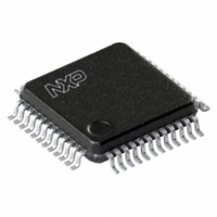
LPC2102FBD48,151 NXP Semiconductors, LPC2102FBD48,151 Datasheet - Page 12

LPC2102FBD48,151
Manufacturer Part Number
LPC2102FBD48,151
Description
IC ARM7 MCU FLASH 16K 48-LQFP
Manufacturer
NXP Semiconductors
Series
LPC2100r
Datasheet
1.LPC2101FBD48151.pdf
(37 pages)
Specifications of LPC2102FBD48,151
Program Memory Type
FLASH
Program Memory Size
16KB (16K x 8)
Package / Case
48-LQFP
Core Processor
ARM7
Core Size
16/32-Bit
Speed
70MHz
Connectivity
I²C, Microwire, SPI, SSI, SSP, UART/USART
Peripherals
POR, PWM, WDT
Number Of I /o
32
Ram Size
4K x 8
Voltage - Supply (vcc/vdd)
1.65 V ~ 3.6 V
Data Converters
A/D 8x10b
Oscillator Type
Internal
Operating Temperature
-40°C ~ 85°C
Processor Series
LPC21
Core
ARM7TDMI-S
Data Bus Width
16 bit, 32 bit
Data Ram Size
4 KB
Interface Type
I2C/JTAG/SPI/SSP/UART
Maximum Clock Frequency
70 MHz
Number Of Programmable I/os
32
Number Of Timers
4
Operating Supply Voltage
3.3 V
Maximum Operating Temperature
+ 85 C
Mounting Style
SMD/SMT
3rd Party Development Tools
MDK-ARM, RL-ARM, ULINK2
Minimum Operating Temperature
- 40 C
On-chip Adc
8-ch x 10-bit
Cpu Family
LPC2000
Device Core
ARM7TDMI-S
Device Core Size
16/32Bit
Frequency (max)
70MHz
Total Internal Ram Size
4KB
# I/os (max)
32
Number Of Timers - General Purpose
4
Operating Supply Voltage (typ)
1.8/3.3V
Operating Supply Voltage (max)
1.95/3.6V
Operating Supply Voltage (min)
1.65/3V
Instruction Set Architecture
RISC
Operating Temp Range
-40C to 85C
Operating Temperature Classification
Industrial
Mounting
Surface Mount
Pin Count
48
Package Type
LQFP
Package
48LQFP
Family Name
LPC2000
Maximum Speed
70 MHz
Lead Free Status / RoHS Status
Lead free / RoHS Compliant
For Use With
568-4310 - EVAL BOARD LPC2158 W/LCD568-4297 - BOARD EVAL LPC21XX MCB2100MCB2103UME - BOARD EVAL MCB2103 + ULINK-MEMCB2103U - BOARD EVAL MCB2103 + ULINK2MCB2103 - BOARD EVAL NXP LPC2101/2101/2103622-1005 - USB IN-CIRCUIT PROG ARM7 LPC2K
Eeprom Size
-
Lead Free Status / Rohs Status
Compliant
Other names
568-2093
935280965151
LPC2102FBD48-S
935280965151
LPC2102FBD48-S
Available stocks
Company
Part Number
Manufacturer
Quantity
Price
Company:
Part Number:
LPC2102FBD48,151
Manufacturer:
NXP Semiconductors
Quantity:
10 000
NXP Semiconductors
LPC2101_02_03_4
Product data sheet
6.5.1 Interrupt sources
6.5 Interrupt controller
6.6 Pin connect block
The VIC accepts all of the interrupt request inputs and categorizes them as FIQ, vectored
IRQ, and non-vectored IRQ as defined by programmable settings. The programmable
assignment scheme means that priorities of interrupts from the various peripherals can be
dynamically assigned and adjusted.
FIQ has the highest priority. If more than one request is assigned to FIQ, the VIC
combines the requests to produce the FIQ signal to the ARM processor. The fastest
possible FIQ latency is achieved when only one request is classified as FIQ, because then
the FIQ service routine does not need to branch into the interrupt service routine but can
run from the interrupt vector location. If more than one request is assigned to the FIQ
class, the FIQ service routine will read a word from the VIC that identifies which FIQ
source(s) is (are) requesting an interrupt.
Vectored IRQs have the middle priority. Sixteen of the interrupt requests can be assigned
to this category. Any of the interrupt requests can be assigned to any of the 16 vectored
IRQ slots, among which slot 0 has the highest priority and slot 15 has the lowest.
Non-vectored IRQs have the lowest priority.
The VIC combines the requests from all the vectored and non-vectored IRQs to produce
the IRQ signal to the ARM processor. The IRQ service routine can start by reading a
register from the VIC and jumping there. If any of the vectored IRQs are pending, the VIC
provides the address of the highest-priority requesting IRQs service routine, otherwise it
provides the address of a default routine that is shared by all the non-vectored IRQs. The
default routine can read another VIC register to see what IRQs are active.
Each peripheral device has one interrupt line connected to the Vectored Interrupt
Controller, but may have several internal interrupt flags. Individual interrupt flags may also
represent more than one interrupt source.
The pin connect block allows selected pins of the microcontroller to have more than one
function. Configuration registers control the multiplexers to allow connection between the
pin and the on chip peripherals. Peripherals should be connected to the appropriate pins
prior to being activated, and prior to any related interrupt(s) being enabled. Activity of any
enabled peripheral function that is not mapped to a related pin should be considered
undefined.
The pin control module with its pin select registers defines the functionality of the
microcontroller in a given hardware environment.
After reset all pins of Port 0 are configured as input with the following exceptions: If the
DBGSEL pin is HIGH (Debug mode enabled), the JTAG pins will assume their JTAG
functionality for use with EmbeddedICE and cannot be configured via the pin connect
block.
Rev. 04 — 2 June 2009
Single-chip 16-bit/32-bit microcontrollers
LPC2101/02/03
© NXP B.V. 2009. All rights reserved.
12 of 37


