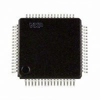
LPC2141FBD64,151 NXP Semiconductors, LPC2141FBD64,151 Datasheet - Page 11

LPC2141FBD64,151
Manufacturer Part Number
LPC2141FBD64,151
Description
IC ARM7 MCU FLASH 32K 64LQFP
Manufacturer
NXP Semiconductors
Series
LPC2100r
Datasheet
1.LPC2141FBD64151.pdf
(40 pages)
Specifications of LPC2141FBD64,151
Program Memory Type
FLASH
Program Memory Size
32KB (32K x 8)
Package / Case
64-LQFP
Core Processor
ARM7
Core Size
16/32-Bit
Speed
60MHz
Connectivity
I²C, Microwire, SPI, SSI, SSP, UART/USART, USB
Peripherals
Brown-out Detect/Reset, POR, PWM, WDT
Number Of I /o
45
Ram Size
8K x 8
Voltage - Supply (vcc/vdd)
3 V ~ 3.6 V
Data Converters
A/D 6x10b
Oscillator Type
Internal
Operating Temperature
-40°C ~ 85°C
Processor Series
LPC21
Core
ARM7TDMI-S
Data Bus Width
16 bit, 32 bit
Data Ram Size
8 KB
Interface Type
SCI/UART/SPI/SSP/I2C/USB
Maximum Clock Frequency
60 MHz
Number Of Programmable I/os
45
Number Of Timers
2
Operating Supply Voltage
3.3 V
Maximum Operating Temperature
+ 85 C
Mounting Style
SMD/SMT
3rd Party Development Tools
MDK-ARM, RL-ARM, ULINK2
Minimum Operating Temperature
- 40 C
On-chip Adc
6-ch x 10-bit
Cpu Family
LPC2000
Device Core
ARM7TDMI-S
Device Core Size
16/32Bit
Frequency (max)
60MHz
Total Internal Ram Size
8KB
# I/os (max)
45
Number Of Timers - General Purpose
2
Operating Supply Voltage (typ)
3.3V
Operating Supply Voltage (max)
3.6V
Operating Supply Voltage (min)
3V
Instruction Set Architecture
RISC
Operating Temp Range
-40C to 85C
Operating Temperature Classification
Industrial
Mounting
Surface Mount
Pin Count
64
Package Type
LQFP
Package
64LQFP
Family Name
LPC2000
Maximum Speed
60 MHz
Lead Free Status / RoHS Status
Lead free / RoHS Compliant
For Use With
568-4310 - EVAL BOARD LPC2158 W/LCD568-4297 - BOARD EVAL LPC21XX MCB2100MCB2140UME - BOARD EVAL MCB2140 + ULINK-MEMCB2140U - BOARD EVAL MCB2140 + ULINK2MCB2140 - BOARD EVAL NXP LPC214X ARM FAM622-1005 - USB IN-CIRCUIT PROG ARM7 LPC2K568-2097 - BOARD EVAL FOR LPC214X ARM MCU
Eeprom Size
-
Lead Free Status / Rohs Status
Compliant
Other names
568-1761
935280015151
LPC2141FBD64-S
935280015151
LPC2141FBD64-S
Available stocks
Company
Part Number
Manufacturer
Quantity
Price
Company:
Part Number:
LPC2141FBD64,151
Manufacturer:
NXP Semiconductors
Quantity:
10 000
NXP Semiconductors
Table 3.
[1]
[2]
[3]
LPC2141_42_44_46_48_4
Product data sheet
Symbol
P1.26/RTCK
P1.27/TDO
P1.28/TDI
P1.29/TCK
P1.30/TMS
P1.31/TRST
D+
D
RESET
XTAL1
XTAL2
RTCX1
RTCX2
V
V
V
V
VREF
VBAT
SS
SSA
DD
DDA
5 V tolerant pad (no built-in pull-up resistor) providing digital I/O functions with TTL levels and hysteresis and 10 ns slew rate control.
5 V tolerant pad (no built-in pull-up resistor) providing digital I/O functions with TTL levels and hysteresis and 10 ns slew rate control. If
configured for an input function, this pad utilizes built-in glitch filter that blocks pulses shorter than 3 ns.
Open-drain 5 V tolerant digital I/O I
functionality.
Pin description
Pin
24
64
60
56
52
20
10
11
57
62
61
3
5
6, 18, 25, 42,
50
59
23, 43, 51
7
63
49
[9]
[9]
[6]
[6]
[6]
[6]
[6]
[6]
[7]
[7]
[8]
[9]
[9]
…continued
Type
I/O
I/O
I/O
O
I/O
I
I/O
I
I/O
I
I/O
I
I/O
I/O
I
I
O
I
O
I
I
I
I
I
I
2
C-bus 400 kHz specification compatible pad. It requires external pull-up to provide an output
Description
P1.26 — General purpose input/output digital pin (GPIO).
RTCK — Returned Test Clock output. Extra signal added to the JTAG port.
Assists debugger synchronization when processor frequency varies.
Bidirectional pin with internal pull-up.
Note: LOW on RTCK while RESET is LOW enables pins P1.31:26 to operate
as Debug port after reset.
P1.27 — General purpose input/output digital pin (GPIO).
TDO — Test Data out for JTAG interface.
P1.28 — General purpose input/output digital pin (GPIO).
TDI — Test Data in for JTAG interface.
P1.29 — General purpose input/output digital pin (GPIO).
TCK — Test Clock for JTAG interface. This clock must be slower than
the CPU clock (CCLK) for the JTAG interface to operate.
P1.30 — General purpose input/output digital pin (GPIO).
TMS — Test Mode Select for JTAG interface.
P1.31 — General purpose input/output digital pin (GPIO).
TRST — Test Reset for JTAG interface.
USB bidirectional D+ line.
USB bidirectional D line.
External reset input: A LOW on this pin resets the device, causing I/O ports
and peripherals to take on their default states, and processor execution to
begin at address 0. TTL with hysteresis, 5 V tolerant.
Input to the oscillator circuit and internal clock generator circuits.
Output from the oscillator amplifier.
Input to the RTC oscillator circuit.
Output from the RTC oscillator circuit.
Ground: 0 V reference.
Analog ground: 0 V reference. This should nominally be the same voltage
as V
3.3 V power supply: This is the power supply voltage for the core and I/O
ports.
Analog 3.3 V power supply: This should be nominally the same voltage as
V
used to power the on-chip ADC(s) and DAC.
ADC reference voltage: This should be nominally less than or equal to the
V
pin is used as a reference for ADC(s) and DAC.
RTC power supply voltage: 3.3 V on this pin supplies the power to the RTC.
DD
DD
Rev. 04 — 17 November 2008
SS
but should be isolated to minimize noise and error. This voltage is only
voltage but should be isolated to minimize noise and error. Level on this
, but should be isolated to minimize noise and error.
LPC2141/42/44/46/48
Single-chip 16-bit/32-bit microcontrollers
© NXP B.V. 2008. All rights reserved.
1
11 of 40
6
of


