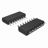
ST62T03CM6 STMicroelectronics, ST62T03CM6 Datasheet - Page 61

ST62T03CM6
Manufacturer Part Number
ST62T03CM6
Description
IC MCU 8BIT W/ADC 16-SOP
Manufacturer
STMicroelectronics
Series
ST6r
Datasheet
1.ST62T03CM6.pdf
(100 pages)
Specifications of ST62T03CM6
Core Processor
ST6
Core Size
8-Bit
Speed
8MHz
Peripherals
LVD, POR, WDT
Number Of I /o
9
Program Memory Size
1KB (1K x 8)
Program Memory Type
OTP
Ram Size
64 x 8
Voltage - Supply (vcc/vdd)
3 V ~ 6 V
Oscillator Type
Internal
Operating Temperature
-40°C ~ 85°C
Package / Case
16-SOIC (0.300", 7.5mm Width)
Controller Family/series
ST6
No. Of I/o's
9
Ram Memory Size
64Byte
Cpu Speed
8MHz
No. Of Timers
2
Rohs Compliant
Yes
Processor Series
ST62T0x
Core
ST6
Data Bus Width
8 bit
Data Ram Size
64 B
Maximum Clock Frequency
8 MHz
Number Of Programmable I/os
9
Number Of Timers
2
Operating Supply Voltage
3 V to 6 V
Maximum Operating Temperature
+ 85 C
Mounting Style
SMD/SMT
Development Tools By Supplier
ST622XC-KIT/110, ST62GP-EMU2, ST62E2XC-EPB/110, ST62E6XC-EPB/US, STREALIZER-II
Minimum Operating Temperature
- 40 C
On-chip Adc
8 bit
Lead Free Status / RoHS Status
Lead free / RoHS Compliant
Eeprom Size
-
Data Converters
-
Connectivity
-
Lead Free Status / Rohs Status
In Transition
Other names
497-8233
ST62T03CM6
ST62T03CM6
Available stocks
Company
Part Number
Manufacturer
Quantity
Price
OPERATING CONDITIONS (Cont’d)
10.3.2 Operating Conditions with Low Voltage Detector (LVD)
Subject to general operating conditions for V
Notes:
1. LVD typical data are based on T
2. The minimum V
3. Data based on characterization results, not tested in production.
Figure 33. LVD Threshold Versus V
Figure 34. Typical LVD Thresholds Versus
Temperature for OTP devices
DEVICE UNDER
V
V
V
Vt
t
Thresholds [V]
4.2
3.8
3.6
g(VDD)
Symbol
IN THIS AREA
IT+
IT-
hys
4
POR
-40°C
RESET
f
OSC
Reset release threshold
(V
Reset generation threshold
(V
LVD voltage threshold hysteresis
V
Filtered glitch delay on V
DD
DD
DD
8
4
0
[MHz]
2.5
rise time rate
DD
rise)
fall)
25°C
rise time rate is needed to insure a correct device power-on and LVD reset. Not tested in production.
Parameter
T [°C]
3
2)
A
95°C
=25°C. They are given only as design guidelines and are not tested.
DD
3.5
3)
V
V
Vdd up
Vdd down
DD
IT+
IT-
V
IT-
and f
3.6
125°C
Doc ID 4563 Rev 5
V
Not detected by the LVD
DD
4
IT+
OSC
, f
-V
OSC
IT-
3)
Conditions
, and T
Figure
Temperature for ROM devices
4.5
Thresholds [V]
4.2
3.8
3.6
4
-40°C
A
.
35.
5
Typical
ST6200C ST6201C ST6203C
25°C
Min
3.9
3.6
5.5
50
T [°C]
LVD
Typ
4.1
3.8
300
30
6
1)
95°C
thresholds
FUNCTIONALITY
NOT GUARANTEED
IN THIS AREA
FUNCTIONAL AREA
SUPPLY
VOLTAGE [V]
Max
4.3
700
V
V
4
Vdd up
Vdd down
IT+
IT-
125°C
mV/s
Unit
61/100
mV
ns
V
vs.
1


