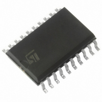
ST62T20CM6 STMicroelectronics, ST62T20CM6 Datasheet - Page 27

ST62T20CM6
Manufacturer Part Number
ST62T20CM6
Description
IC MCU 8BIT OTP 4K 20 SOIC
Manufacturer
STMicroelectronics
Series
ST6r
Datasheet
1.ST62T10CB6.pdf
(104 pages)
Specifications of ST62T20CM6
Core Processor
ST6
Core Size
8-Bit
Speed
8MHz
Peripherals
LVD, POR, WDT
Number Of I /o
12
Program Memory Size
4KB (4K x 8)
Program Memory Type
OTP
Ram Size
64 x 8
Voltage - Supply (vcc/vdd)
3 V ~ 6 V
Data Converters
A/D 8x8b
Oscillator Type
Internal
Operating Temperature
-40°C ~ 85°C
Package / Case
20-SOIC (7.5mm Width)
Controller Family/series
ST6
No. Of I/o's
12
Ram Memory Size
64Byte
Cpu Speed
8MHz
No. Of Timers
2
Rohs Compliant
Yes
Processor Series
ST62T2x
Core
ST6
Data Bus Width
8 bit
Data Ram Size
64 B
Maximum Clock Frequency
8 MHz
Number Of Programmable I/os
12
Number Of Timers
2
Operating Supply Voltage
3 V to 6 V
Maximum Operating Temperature
+ 85 C
Mounting Style
SMD/SMT
Development Tools By Supplier
ST622XC-KIT/110, ST62GP-EMU2, ST62E2XC-EPB/110, ST62E6XC-EPB/US, STREALIZER-II
Minimum Operating Temperature
- 40 C
On-chip Adc
8 bit
Lead Free Status / RoHS Status
Lead free / RoHS Compliant
Eeprom Size
-
Connectivity
-
Lead Free Status / Rohs Status
Details
Other names
497-2099-5
Available stocks
Company
Part Number
Manufacturer
Quantity
Price
5.4 INTERRUPTS
The ST6 core may be interrupted by four maska-
ble interrupt sources, in addition to a Non Maska-
ble Interrupt (NMI) source. The interrupt process-
ing flowchart is shown in
Maskable interrupts must be enabled by setting
the GEN bit in the IOR register. However, even if
they are disabled (GEN bit = 0), interrupt events
are latched and may be processed as soon as the
GEN bit is set.
Each source is associated with a specific Interrupt
Vector, located in Program space (see
the vector location, the user must write a Jump in-
Figure 17. Interrupts Block Diagram
PB0...PB7
PA0...PA3
* Depending on device. See device summary on page 1.
NMI
I/O PORT REGISTER
“INPUT WITH INTERRUPT”
CONFIGURATION
CONFIGURATION
I/O PORT REGISTER
“INPUT WITH INTERRUPT”
A/D CONVERTER *
V D D
Figure
TIMER
(ADCR REGISTER)
(TSCR REGISTER)
18.
(IOR REGISTER)
LATCH
EOC BIT
TMZ BIT
EAI BIT
ETI BIT
Table
AT START OF VECTOR #0 ROUTINE
CLEARED BY H/W
CLEARED BY H/W
AT START OF
VECTOR #1 ROUTINE
ESB BIT
8). In
LATCH
BY H/W AT START OF
VECTOR #2 ROUTINE
CLEARED
struction to the associated interrupt service rou-
tine.
When an interrupt source generates an interrupt
request, the PC register is loaded with the address
of the interrupt vector, which then causes a Jump
to the relevant interrupt service routine, thus serv-
icing the interrupt.
Interrupt are triggered by events either on external
pins, or from the on-chip peripherals. Several
events can be ORed on the same interrupt vector.
On-chip peripherals have flag registers to deter-
mine which event triggered the interrupt.
LATCH
(IOR REGISTER)
ST6208C/ST6209C/ST6210C/ST6220C
(IOR REGISTER)
LES BIT
0
1
GEN BIT
VECTOR #0
VECTOR #1
VECTOR #3
VECTOR #4
VECTOR #2
EXIT FROM
STOP/WAIT
27/104
1


