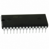
ST62T25CB6 STMicroelectronics, ST62T25CB6 Datasheet - Page 81

ST62T25CB6
Manufacturer Part Number
ST62T25CB6
Description
IC MCU 8BIT OTP 4K 28 PDIP
Manufacturer
STMicroelectronics
Series
ST6r
Specifications of ST62T25CB6
Core Processor
ST6
Core Size
8-Bit
Speed
8MHz
Peripherals
LVD, POR, WDT
Number Of I /o
20
Program Memory Size
4KB (4K x 8)
Program Memory Type
OTP
Ram Size
64 x 8
Voltage - Supply (vcc/vdd)
3 V ~ 6 V
Data Converters
A/D 16x8b
Oscillator Type
Internal
Operating Temperature
-40°C ~ 85°C
Package / Case
28-DIP (0.600", 15.24mm)
Processor Series
ST62T2x
Core
ST6
Data Bus Width
8 bit
Data Ram Size
64 B
Maximum Clock Frequency
8 MHz
Number Of Programmable I/os
20
Number Of Timers
1
Operating Supply Voltage
3 V to 6 V
Maximum Operating Temperature
+ 85 C
Mounting Style
Through Hole
Development Tools By Supplier
ST62GP-EMU2, ST62E2XC-EPB/110, ST62E6XC-EPB/US, ST622XC-KIT/110, STREALIZER-II
Minimum Operating Temperature
- 40 C
On-chip Adc
16-ch x 8-bit
Lead Free Status / RoHS Status
Lead free / RoHS Compliant
Eeprom Size
-
Connectivity
-
Lead Free Status / Rohs Status
Lead free / RoHS Compliant
Other names
497-2100-5
Available stocks
Company
Part Number
Manufacturer
Quantity
Price
Company:
Part Number:
ST62T25CB6
Manufacturer:
ST
Quantity:
310
Company:
Part Number:
ST62T25CB6
Manufacturer:
STMicroelectronics
Quantity:
5
EMC CHARACTERISTICS (Cont’d)
11.7.3 ESD Pin Protection Strategy
To protect an integrated circuit against Electro-
Static Discharge the stress must be controlled to
prevent degradation or destruction of the circuit el-
ements. The stress generally affects the circuit el-
ements which are connected to the pads but can
also affect the internal devices when the supply
pads receive the stress. The elements to be pro-
tected must not receive excessive current, voltage
or heating within their structure.
An ESD network combines the different input and
output ESD protections. This network works, by al-
lowing safe discharge paths for the pins subjected
to ESD stress. Two critical ESD stress cases are
presented in
pins.
Figure 59. Positive Stress on a Standard Pad vs. V
Figure 60. Negative Stress on a Standard Pad vs. V
Main path
Path to avoid
Main path
Figure 59
V
V
V
V
DD
DD
SS
SS
and
Figure 60
(3a)
(3b)
(3a)
(3b)
for standard
OUT
OUT
SS
Standard Pin Protection
To protect the output structure the following ele-
ments are added:
– A diode to V
– A protection device between V
To protect the input structure the following ele-
ments are added:
– A resistor in series with the pad (1)
– A diode to V
– A protection device between V
DD
(4)
(4)
ST6215CM-Auto ST6225CM-Auto
IN
IN
DD
DD
(3a) and a diode from V
(2a) and a diode from V
(2a)
(2b)
(2a)
(2b)
(1)
(1)
DD
DD
and V
and V
SS
SS
SS
SS
81/100
V
V
V
V
(3b)
(2b)
(4)
(4)
DD
SS
DD
SS
1


