MC908QB8CDWE Freescale Semiconductor, MC908QB8CDWE Datasheet - Page 27
MC908QB8CDWE
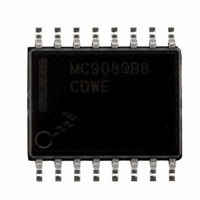
Manufacturer Part Number
MC908QB8CDWE
Description
IC MCU 8BIT 8K FLASH 16-SOIC
Manufacturer
Freescale Semiconductor
Series
HC08r
Datasheet
1.MC908QB8CDWE.pdf
(236 pages)
Specifications of MC908QB8CDWE
Core Processor
HC08
Core Size
8-Bit
Speed
8MHz
Connectivity
SCI, SPI
Peripherals
LVD, POR, PWM
Number Of I /o
13
Program Memory Size
8KB (8K x 8)
Program Memory Type
FLASH
Ram Size
256 x 8
Voltage - Supply (vcc/vdd)
2.7 V ~ 5.5 V
Data Converters
A/D 10x10b
Oscillator Type
Internal
Operating Temperature
-40°C ~ 85°C
Package / Case
16-SOIC (0.300", 7.5mm Width)
Processor Series
HC08QB
Core
HC08
Data Bus Width
8 bit
Data Ram Size
256 B
Interface Type
SCI, SPI
Maximum Clock Frequency
8 MHz
Number Of Programmable I/os
14
Number Of Timers
4
Operating Supply Voltage
3 V to 5 V
Maximum Operating Temperature
+ 85 C
Mounting Style
SMD/SMT
Development Tools By Supplier
FSICEBASE, M68CBL05AE, DEMO908QB8, DEMO908QC16
Minimum Operating Temperature
- 40 C
On-chip Adc
10 bit
For Use With
DEMO908QB8 - BOARD DEMO FOR MC68HC908QB8
Lead Free Status / RoHS Status
Lead free / RoHS Compliant
Eeprom Size
-
Lead Free Status / Rohs Status
Details
Available stocks
Company
Part Number
Manufacturer
Quantity
Price

Part Number:
MC908QB8CDWE
Manufacturer:
FREESCALE
Quantity:
20 000
Part Number:
MC908QB8CDWER
Manufacturer:
FREESCALE
Quantity:
20 000


Freescale Semiconductor
$0022
$0023
$0024
$0025
$0026
$0027
$0028
$0029
$002A
$002B
$002F
$0030
$0031
$0032
$0033
$0034
$0035
Addr.
↓
TIM Counter Register Low
TIM Channel 0 Status and
TIM Channel 1 Status and
TIM Channel 2 Status and
TIM Channel 3 Status and
Control Register (TSC0)
Control Register (TSC1)
Control Register (TSC2)
Control Register (TSC3)
Register High (TMODH)
Register High (TCH0H)
Register High (TCH1H)
Register High (TCH2H)
Register High (TCH3H)
Register Low (TMODL)
Register Low (TCH0L)
Register Low (TCH1L)
Register Low (TCH2L)
Register Low (TCH3L)
Register Name
TIM Counter Modulo
TIM Counter Modulo
TIM Channel 0
TIM Channel 0
TIM Channel 1
TIM Channel 1
TIM Channel 2
TIM Channel 2
TIM Channel 3
TIM Channel 3
See page 185.
See page 185.
See page 185.
See page 186.
See page 189.
See page 189.
See page 186.
See page 189.
See page 189.
See page 186.
See page 189.
See page 189.
See page 186.
See page 189.
See page 189.
Reserved
Figure 2-2. Control, Status, and Data Registers (Sheet 3 of 5)
(TCNTL)
Reset:
Reset:
Reset:
Reset:
Reset:
Reset:
Reset:
Reset:
Reset:
Reset:
Reset:
Reset:
Reset:
Reset:
Reset:
Read:
Read:
Read:
Read:
Read:
Read:
Read:
Read:
Read:
Read:
Read:
Read:
Read:
Read:
Read:
Write:
Write:
Write:
Write:
Write:
Write:
Write:
Write:
Write:
Write:
Write:
Write:
Write:
Write:
Write:
CH0F
CH1F
CH2F
CH3F
Bit 15
Bit 15
Bit 15
Bit 15
Bit 15
Bit 7
Bit 7
Bit 7
Bit 7
Bit 7
Bit 7
Bit 7
0
1
1
0
0
0
0
0
0
0
0
MC68HC908QB8 Data Sheet, Rev. 3
= Unimplemented
CH0IE
CH1IE
CH2IE
CH3IE
Bit 14
Bit 14
Bit 14
Bit 14
Bit 14
Bit 6
Bit 6
Bit 6
Bit 6
Bit 6
Bit 6
6
0
1
1
0
0
0
0
MS0B
Bit 13
Bit 13
Bit 13
Bit 13
Bit 13
Bit 5
Bit 5
Bit 5
Bit 5
Bit 5
Bit 5
5
0
1
1
0
0
0
0
0
0
0
Indeterminate after reset
Indeterminate after reset
Indeterminate after reset
Indeterminate after reset
Indeterminate after reset
Indeterminate after reset
Indeterminate after reset
Indeterminate after reset
MS0A
MS1A
MS2A
MS3A
Bit 12
Bit 12
Bit 12
Bit 12
Bit 12
Bit 4
Bit 4
Bit 4
Bit 4
Bit 4
Bit 4
R
4
0
1
1
0
0
0
0
= Reserved
ELS0B
ELS1B
ELS2B
ELS3B
Bit 11
Bit 11
Bit 11
Bit 11
Bit 11
Bit 3
Bit 3
Bit 3
Bit 3
Bit 3
Bit 3
3
0
1
1
0
0
0
0
ELS0A
ELS1A
ELS2A
ELS3A
Bit 10
Bit 10
Bit 10
Bit 10
Bit 10
U = Unaffected
Bit 2
Bit 2
Bit 2
Bit 2
Bit 2
Bit 2
2
0
1
1
0
0
0
0
Direct Page Registers
TOV0
TOV1
TOV2
TOV3
Bit 1
Bit 9
Bit 1
Bit 9
Bit 1
Bit 9
Bit 1
Bit 9
Bit 1
Bit 9
Bit 1
1
0
1
1
0
0
0
0
CH0MAX
CH1MAX
CH2MAX
CH3MAX
Bit 0
Bit 0
Bit 8
Bit 0
Bit 8
Bit 0
Bit 8
Bit 0
Bit 8
Bit 0
Bit 8
Bit 0
0
1
1
0
0
0
0
27
Related parts for MC908QB8CDWE
Image
Part Number
Description
Manufacturer
Datasheet
Request
R

Part Number:
Description:
Manufacturer:
Freescale Semiconductor, Inc
Datasheet:
Part Number:
Description:
Manufacturer:
Freescale Semiconductor, Inc
Datasheet:
Part Number:
Description:
Manufacturer:
Freescale Semiconductor, Inc
Datasheet:
Part Number:
Description:
Manufacturer:
Freescale Semiconductor, Inc
Datasheet:
Part Number:
Description:
Manufacturer:
Freescale Semiconductor, Inc
Datasheet:
Part Number:
Description:
Manufacturer:
Freescale Semiconductor, Inc
Datasheet:
Part Number:
Description:
Manufacturer:
Freescale Semiconductor, Inc
Datasheet:
Part Number:
Description:
Manufacturer:
Freescale Semiconductor, Inc
Datasheet:
Part Number:
Description:
Manufacturer:
Freescale Semiconductor, Inc
Datasheet:
Part Number:
Description:
Manufacturer:
Freescale Semiconductor, Inc
Datasheet:
Part Number:
Description:
Manufacturer:
Freescale Semiconductor, Inc
Datasheet:
Part Number:
Description:
Manufacturer:
Freescale Semiconductor, Inc
Datasheet:
Part Number:
Description:
Manufacturer:
Freescale Semiconductor, Inc
Datasheet:
Part Number:
Description:
Manufacturer:
Freescale Semiconductor, Inc
Datasheet:
Part Number:
Description:
Manufacturer:
Freescale Semiconductor, Inc
Datasheet: