R5F21256SNFP#U0 Renesas Electronics America, R5F21256SNFP#U0 Datasheet - Page 106
R5F21256SNFP#U0
Manufacturer Part Number
R5F21256SNFP#U0
Description
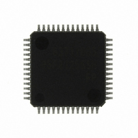
IC R8C MCU FLASH 32K 52LQFP
Manufacturer
Renesas Electronics America
Series
R8C/2x/25r
Datasheets
1.R5F211A2SPU0.pdf
(300 pages)
2.R5F21246SDFPU0.pdf
(61 pages)
3.R5F21246SDFPU0.pdf
(527 pages)
Specifications of R5F21256SNFP#U0
Core Processor
R8C
Core Size
16/32-Bit
Speed
20MHz
Connectivity
I²C, LIN, SIO, SSU, UART/USART
Peripherals
POR, Voltage Detect, WDT
Number Of I /o
41
Program Memory Size
32KB (32K x 8)
Program Memory Type
FLASH
Ram Size
2K x 8
Voltage - Supply (vcc/vdd)
2.2 V ~ 5.5 V
Data Converters
A/D 12x10b
Oscillator Type
Internal
Operating Temperature
-20°C ~ 85°C
Package / Case
52-LQFP
For Use With
R0K521256S000BE - KIT EVAL STARTER FOR R8C/25
Lead Free Status / RoHS Status
Lead free / RoHS Compliant
Eeprom Size
-
Available stocks
Company
Part Number
Manufacturer
Quantity
Price

Part Number:
R5F21256SNFP#U0R5F21256SNFP#ES
Manufacturer:
Renesas Electronics America
Quantity:
10 000


Rev.2.00 Oct 17, 2005
REJ09B0001-0200
LDCTX
[ Syntax ]
[ Function ]
[ Flag Change ]
[ Description Example ]
[ Related Instructions ]
Change
Chapter 3
LDCTX
Flag
• The table data is configured as shown below. The address indicated by abs20 is the base address of
• This instruction restores task context from the stack area.
• Set the RAM address that contains the task number in abs16 and the start address of table data in abs20.
• The required register information is specified from table data by the task number and the data in the
• Information on transferred registers is configured as shown below. Logical 1 indicates a register to be
LDCTX
abs20
the table. The data stored at an address twice the content of abs16 away from the base address
indicates register information, and the next address contains the stack pointer correction value.
stack area is transferred to each register according to the specified register information. Then the SP
correction value is added to the stack pointer (SP). For this SP correction value, set the number of
bytes to be transferred.
transferred and logical 0 indicates a register that is not transferred.
U
I
Direction in
which address
increases
Base address
of table
abs16,abs20
Ram,Rom_TBL
Functions
O
page 86 of 263
B
S
STCTX
*1
Z
Register information for task with task number n
SP correction value for task with task number n
Register information for task with task number 0. (See above diagram.)
Register information for task with task number 1. (See above diagram.)
SP correction value for task with task number 0. (See above diagram.)
SP correction value for task with task number 1. (See above diagram.)
MSB
D
n=0 to 255
FB SB A1 A0 R3 R2 R1 R0
C
Transferred sequentially
beginning with R0
LoaD ConTeXt
Restore context
[ Instruction Code/Number of Cycles ]
LSB
*1
*1
. (See above diagram.)
. (See above diagram.)
LDCTX
3.2 Functions
Page: 189
abs16 2
Related parts for R5F21256SNFP#U0
Image
Part Number
Description
Manufacturer
Datasheet
Request
R

Part Number:
Description:
KIT STARTER FOR M16C/29
Manufacturer:
Renesas Electronics America
Datasheet:

Part Number:
Description:
KIT STARTER FOR R8C/2D
Manufacturer:
Renesas Electronics America
Datasheet:

Part Number:
Description:
R0K33062P STARTER KIT
Manufacturer:
Renesas Electronics America
Datasheet:

Part Number:
Description:
KIT STARTER FOR R8C/23 E8A
Manufacturer:
Renesas Electronics America
Datasheet:

Part Number:
Description:
KIT STARTER FOR R8C/25
Manufacturer:
Renesas Electronics America
Datasheet:

Part Number:
Description:
KIT STARTER H8S2456 SHARPE DSPLY
Manufacturer:
Renesas Electronics America
Datasheet:

Part Number:
Description:
KIT STARTER FOR R8C38C
Manufacturer:
Renesas Electronics America
Datasheet:

Part Number:
Description:
KIT STARTER FOR R8C35C
Manufacturer:
Renesas Electronics America
Datasheet:

Part Number:
Description:
KIT STARTER FOR R8CL3AC+LCD APPS
Manufacturer:
Renesas Electronics America
Datasheet:
Part Number:
Description:
KIT STARTER FOR RX610
Manufacturer:
Renesas Electronics America
Datasheet:

Part Number:
Description:
KIT STARTER FOR R32C/118
Manufacturer:
Renesas Electronics America
Datasheet:

Part Number:
Description:
KIT DEV RSK-R8C/26-29
Manufacturer:
Renesas Electronics America
Datasheet:

Part Number:
Description:
KIT STARTER FOR SH7124
Manufacturer:
Renesas Electronics America
Datasheet:

Part Number:
Description:
KIT STARTER FOR H8SX/1622
Manufacturer:
Renesas Electronics America
Datasheet:

Part Number:
Description:
KIT DEV FOR SH7203
Manufacturer:
Renesas Electronics America
Datasheet: