R5F21276SNFP#U0 Renesas Electronics America, R5F21276SNFP#U0 Datasheet
R5F21276SNFP#U0
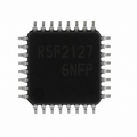
Specifications of R5F21276SNFP#U0
Available stocks


Related parts for R5F21276SNFP#U0


R5F21276SNFP#U0 Summary of contents
Page 1
To our customers, Old Company Name in Catalogs and Other Documents st On April 1 , 2010, NEC Electronics Corporation merged with Renesas Technology Corporation, and Renesas Electronics Corporation took over all the business of both companies. Therefore, although the ...
Page 2
All information included in this document is current as of the date this document is issued. Such information, however, is subject to change without any prior notice. Before purchasing or using any Renesas Electronics products listed herein, please confirm ...
Page 3
R8C/26 Group, R8C/27 Group SINGLE-CHIP 16-BIT CMOS MCU 1. Overview These MCUs are fabricated using a high-performance silicon gate CMOS process, embedding the R8C CPU core, and are packaged in a 32-pin molded-plastic LQFP. It implements sophisticated instructions for a ...
Page 4
R8C/26 Group, R8C/27 Group 1.2 Performance Overview Table 1.1 outlines the Functions and Specifications for R8C/26 Group and Table 1.2 outlines the Functions and Specifications for R8C/27 Group. Table 1.1 Functions and Specifications for R8C/26 Group Item CPU Number of ...
Page 5
R8C/26 Group, R8C/27 Group Table 1.2 Functions and Specifications for R8C/27 Group Item CPU Number of fundamental instructions Minimum instruction execution time Operating mode Address space Memory capacity Peripheral Ports Functions LED drive ports Timers Serial interfaces Clock synchronous serial ...
Page 6
R8C/26 Group, R8C/27 Group 1.3 Block Diagram Figure 1.1 shows a Block Diagram. I/O ports Peripheral functions Timers Timer RA (8 bits) Timer RB (8 bits) Timer RC (16 bits × 1 channel) Timer RE (8 bits) Watchdog timer (15 ...
Page 7
R8C/26 Group, R8C/27 Group 1.4 Product Information Table 1.3 lists the Product Information for R8C/26 Group and Table 1.4 lists the Product Information for R8C/27 Group. Table 1.3 Product Information for R8C/26 Group Part No. R5F21262SNFP R5F21264SNFP R5F21265SNFP R5F21266SNFP R5F21262SDFP ...
Page 8
R8C/26 Group, R8C/27 Group Part No XXX FP Figure 1.2 Part Number, Memory Size, and Package of R8C/26 Group Rev.2.10 Sep 26, 2008 Page REJ03B0168-0210 Package type: FP: PLQP0032GB-A ...
Page 9
R8C/26 Group, R8C/27 Group Table 1.4 Product Information for R8C/27 Group Part No. Program ROM R5F21272SNFP 8 Kbytes 1 Kbyte × 2 512 bytes R5F21274SNFP 16 Kbytes 1 Kbyte × Kbyte R5F21275SNFP 24 Kbytes 1 Kbyte × 2 ...
Page 10
R8C/26 Group, R8C/27 Group Part No XXX FP Figure 1.3 Part Number, Memory Size, and Package of R8C/27 Group Rev.2.10 Sep 26, 2008 Page REJ03B0168-0210 Package type: FP: PLQP0032GB-A ...
Page 11
R8C/26 Group, R8C/27 Group 1.5 Pin Assignments Figure 1.4 shows Pin Assignments (Top View). P0_7/AN0 P0_6/AN1 P0_5/AN2/CLK1 P0_4/AN3/TREO P0_3/AN4 P0_2/AN5 P0_1/AN6 (2) P0_0/AN7/(TXD1) NOTES: 1. P4_7 is an input-only port. 2. Can be assigned to the pin in parentheses by ...
Page 12
R8C/26 Group, R8C/27 Group 1.6 Pin Functions Table 1.5 lists Pin Functions. Table 1.5 Pin Functions Type Symbol Power supply input VCC, VSS Analog power AVCC, AVSS supply input Reset input RESET MODE MODE XIN clock input XIN XIN clock ...
Page 13
R8C/26 Group, R8C/27 Group Table 1.6 Pin Name Information by Pin Number Pin Control Pin Number RESET 4 (2) XOUT/XCOUT 5 VSS/AVSS 6 (2) XIN/XCIN 7 VCC/AVCC 8 MODE ...
Page 14
R8C/26 Group, R8C/27 Group 2. Central Processing Unit (CPU) Figure 2.1 shows the CPU Registers. The CPU contains 13 registers. R0, R1, R2, R3, A0, A1, and FB configure a register bank. There are two sets of register bank. b31 ...
Page 15
R8C/26 Group, R8C/27 Group 2.1 Data Registers (R0, R1, R2, and R3 16-bit register for transfer, arithmetic, and logic operations. The same applies R3. R0 can be split into high-order bits (R0H) and low-order ...
Page 16
R8C/26 Group, R8C/27 Group 2.8.7 Interrupt Enable Flag (I) The I flag enables maskable interrupts. Interrupt are disabled when the I flag is set to 0, and are enabled when the I flag is set to 1. The I flag ...
Page 17
R8C/26 Group, R8C/27 Group 3. Memory 3.1 R8C/26 Group Figure 3 Memory Map of R8C/26 Group. The R8C/26 group has 1 Mbyte of address space from addresses 00000h to FFFFFh. The internal ROM is allocated lower addresses, beginning ...
Page 18
R8C/26 Group, R8C/27 Group 3.2 R8C/27 Group Figure 3 Memory Map of R8C/27 Group. The R8C/27 group has 1 Mbyte of address space from addresses 00000h to FFFFFh. The internal ROM (program ROM) is allocated lower addresses, beginning ...
Page 19
R8C/26 Group, R8C/27 Group 4. Special Function Registers (SFRs) An SFR (special function register control register for a peripheral function. Tables 4.1 to 4.7 list the special function registers. Table 4.1 SFR Information (1) Address 0000h 0001h 0002h ...
Page 20
R8C/26 Group, R8C/27 Group Table 4.2 SFR Information (2) Address 0030h 0031h Voltage Detection Register 1 0032h Voltage Detection Register 2 0033h 0034h 0035h 0036h Voltage Monitor 1 Circuit Control Register 0037h Voltage Monitor 2 Circuit Control Register 0038h Voltage ...
Page 21
R8C/26 Group, R8C/27 Group Table 4.3 SFR Information (3) Address 0080h 0081h 0082h 0083h 0084h 0085h 0086h 0087h 0088h 0089h 008Ah 008Bh 008Ch 008Dh 008Eh 008Fh 0090h 0091h 0092h 0093h 0094h 0095h 0096h 0097h 0098h 0099h 009Ah 009Bh 009Ch 009Dh ...
Page 22
R8C/26 Group, R8C/27 Group Table 4.4 SFR Information (4) Address 00C0h A/D Register 00C1h 00C2h 00C3h 00C4h 00C5h 00C6h 00C7h 00C8h 00C9h 00CAh 00CBh 00CCh 00CDh 00CEh 00CFh 00D0h 00D1h 00D2h 00D3h 00D4h A/D Control Register 2 00D5h 00D6h A/D ...
Page 23
R8C/26 Group, R8C/27 Group Table 4.5 SFR Information (5) Address 0100h Timer RA Control Register 0101h Timer RA I/O Control Register 0102h Timer RA Mode Register 0103h Timer RA Prescaler Register 0104h Timer RA Register 0105h 0106h LIN Control Register ...
Page 24
R8C/26 Group, R8C/27 Group Table 4.6 SFR Information (6) Address 0140h 0141h 0142h 0143h 0144h 0145h 0146h 0147h 0148h 0149h 014Ah 014Bh 014Ch 014Dh 014Eh 014Fh 0150h 0151h 0152h 0153h 0154h 0155h 0156h 0157h 0158h 0159h 015Ah 015Bh 015Ch 015Dh ...
Page 25
R8C/26 Group, R8C/27 Group Table 4.7 SFR Information (7) Address 0180h 0181h 0182h 0183h 0184h 0185h 0186h 0187h 0188h 0189h 018Ah 018Bh 018Ch 018Dh 018Eh 018Fh 0190h 0191h 0192h 0193h 0194h 0195h 0196h 0197h 0198h 0199h 019Ah 019Bh 019Ch 019Dh ...
Page 26
R8C/26 Group, R8C/27 Group 5. Electrical Characteristics 5 Version Table 5.1 Absolute Maximum Ratings Symbol Parameter V /AV Supply voltage Input voltage I V Output voltage O P Power dissipation d T Operating ambient temperature ...
Page 27
R8C/26 Group, R8C/27 Group Table 5.3 A/D Converter Characteristics Symbol Parameter − Resolution − Absolute 10-bit mode accuracy 8-bit mode 10-bit mode 8-bit mode 10-bit mode 8-bit mode R Resistor ladder ladder t Conversion time 10-bit mode conv 8-bit mode ...
Page 28
R8C/26 Group, R8C/27 Group Table 5.4 Flash Memory (Program ROM) Electrical Characteristics Symbol Parameter − Program/erase endurance − Byte program time − Block erase time t Time delay from suspend request until d(SR-SUS) suspend − Interval from erase start/restart until ...
Page 29
R8C/26 Group, R8C/27 Group Table 5.5 Flash Memory (Data flash Block A, Block B) Electrical Characteristics Symbol Parameter − Program/erase endurance − Byte program time (program/erase endurance ≤ 1,000 times) − Byte program time (program/erase endurance > 1,000 times) − ...
Page 30
R8C/26 Group, R8C/27 Group Suspend request (maskable interrupt request) FMR46 Figure 5.2 Time delay until Suspend Table 5.6 Voltage Detection 0 Circuit Electrical Characteristics Symbol V Voltage detection level det0 − Voltage detection circuit self power consumption t Waiting time ...
Page 31
R8C/26 Group, R8C/27 Group Table 5.9 Power-on Reset Circuit, Voltage Monitor 0 Reset Electrical Characteristics Symbol Parameter V Power-on reset valid voltage por1 V Power-on reset or voltage monitor 0 reset valid por2 voltage t External power V rth CC ...
Page 32
R8C/26 Group, R8C/27 Group Table 5.10 High-speed On-Chip Oscillator Circuit Electrical Characteristics Symbol Parameter fOCO40M High-speed on-chip oscillator frequency temperature • supply voltage dependence High-speed on-chip oscillator frequency when correction value in FRA7 register is written to (4) FRA1 register ...
Page 33
R8C/26 Group, R8C/27 Group Table 5.13 Timing Requirements of Clock Synchronous Serial I/O with Chip Select Symbol Parameter t SSCK clock cycle time SUCYC t SSCK clock “H” width HI t SSCK clock “L” width LO t SSCK clock rising ...
Page 34
R8C/26 Group, R8C/27 Group 4-Wire Bus Communication Mode, Master, CPHS = SCS (output) SSCK (output) (CPOS = 1) SSCK (output) (CPOS = 0) SSO (output) SSI (input 4-Wire Bus Communication Mode, Master, CPHS = 0 ...
Page 35
R8C/26 Group, R8C/27 Group 4-Wire Bus Communication Mode, Slave, CPHS = 1 SCS (input) SSCK (input) (CPOS = 1) SSCK (input) (CPOS = 0) SSO (input) SSI (output) 4-Wire Bus Communication Mode, Slave, CPHS = 0 SCS (input) SSCK (input) ...
Page 36
R8C/26 Group, R8C/27 Group SSCK SSO (output) SSI (input) Figure 5.6 I/O Timing of Clock Synchronous Serial I/O with Chip Select (Clock Synchronous Communication Mode) Rev.2.10 Sep 26, 2008 Page 34 ...
Page 37
R8C/26 Group, R8C/27 Group Table 5.14 Timing Requirements of I Symbol Parameter t SCL input cycle time SCL t SCL input “H” width SCLH t SCL input “L” width SCLL t SCL, SDA input fall time sf t SCL, SDA ...
Page 38
R8C/26 Group, R8C/27 Group Table 5.15 Electrical Characteristics (1) [V Symbol Parameter V Output “H” voltage Except P1_0 to P1_7, OH XOUT P1_0 to P1_7 XOUT V Output “L” voltage Except P1_0 to P1_7, OL XOUT P1_0 to P1_7 XOUT ...
Page 39
R8C/26 Group, R8C/27 Group Table 5.16 Electrical Characteristics (2) [Vcc = -20 to 85°C (N version) / -40 to 85°C (D version), unless otherwise specified.) opr Symbol Parameter I Power supply current High-speed ...
Page 40
R8C/26 Group, R8C/27 Group Table 5.17 Electrical Characteristics (3) [Vcc = -20 to 85°C (N version) / -40 to 85°C (D version), unless otherwise specified.) opr Symbol Parameter I Power supply current Wait mode CC (V ...
Page 41
R8C/26 Group, R8C/27 Group Timing Requirements (Unless Otherwise Specified: V Table 5.18 XIN Input, XCIN Input Symbol t XIN input cycle time c(XIN) t XIN input “H” width WH(XIN) t XIN input “L” width WL(XIN) t XCIN input cycle time ...
Page 42
R8C/26 Group, R8C/27 Group Table 5.20 Serial Interface Symbol t CLKi input cycle time c(CK) t CLKi input “H” width W(CKH) t CLKi input “L” width W(CKL) t TXDi output delay time d(C-Q) t TXDi hold time h(C-Q) t RXDi ...
Page 43
R8C/26 Group, R8C/27 Group Table 5.22 Electrical Characteristics (3) [V Symbol Parameter V Output “H” voltage Except P1_0 to P1_7, OH XOUT P1_0 to P1_7 XOUT V Output “L” voltage Except P1_0 to P1_7, OL XOUT P1_0 to P1_7 XOUT ...
Page 44
R8C/26 Group, R8C/27 Group Table 5.23 Electrical Characteristics (4) [Vcc = -20 to 85°C (N version) / -40 to 85°C (D version), unless otherwise specified.) opr Symbol Parameter I Power supply current High-speed ...
Page 45
R8C/26 Group, R8C/27 Group Timing requirements (Unless Otherwise Specified: V Table 5.24 XIN Input, XCIN Input Symbol t XIN input cycle time c(XIN) t XIN input “H” width WH(XIN) t XIN input “L” width WL(XIN) t XCIN input cycle time ...
Page 46
R8C/26 Group, R8C/27 Group Table 5.26 Serial Interface Symbol t CLKi input cycle time c(CK) t CLKi input “H” width W(CKH) t CLKi Input “L” width W(CKL) t TXDi output delay time d(C-Q) t TXDi hold time h(C-Q) t RXDi ...
Page 47
R8C/26 Group, R8C/27 Group Table 5.28 Electrical Characteristics (5) [V Symbol Parameter V Output “H” voltage Except P1_0 to P1_7, OH XOUT P1_0 to P1_7 XOUT V Output “L” voltage Except P1_0 to P1_7, OL XOUT P1_0 to P1_7 XOUT ...
Page 48
R8C/26 Group, R8C/27 Group Table 5.29 Electrical Characteristics (6) [Vcc = 2 -20 to 85°C (N version) / -40 to 85°C (D version), unless otherwise specified.) opr Symbol Parameter I Power supply current High-speed ...
Page 49
R8C/26 Group, R8C/27 Group Timing requirements (Unless Otherwise Specified: V Table 5.30 XIN Input, XCIN Input Symbol t XIN input cycle time c(XIN) t XIN input “H” width WH(XIN) t XIN input “L” width WL(XIN) t XCIN input cycle time ...
Page 50
R8C/26 Group, R8C/27 Group Table 5.32 Serial Interface Symbol t CLKi input cycle time c(CK) t CLKi input “H” width W(CKH) t CLKi input “L” width W(CKL) t TXDi output delay time d(C-Q) t TXDi hold time h(C-Q) t RXDi ...
Page 51
R8C/26 Group, R8C/27 Group 5 Version Table 5.34 Absolute Maximum Ratings Symbol Parameter V /AV Supply voltage Input voltage I V Output voltage O P Power dissipation d T Operating ambient temperature opr T Storage ...
Page 52
R8C/26 Group, R8C/27 Group Table 5.36 A/D Converter Characteristics Symbol Parameter − Resolution − Absolute 10-bit mode accuracy 8-bit mode 10-bit mode 8-bit mode R Resistor ladder ladder t Conversion time 10-bit mode conv 8-bit mode V Reference voltage ref ...
Page 53
R8C/26 Group, R8C/27 Group Table 5.37 Flash Memory (Program ROM) Electrical Characteristics Symbol Parameter − Program/erase endurance − Byte program time − Block erase time t Time delay from suspend request until d(SR-SUS) suspend − Interval from erase start/restart until ...
Page 54
R8C/26 Group, R8C/27 Group Table 5.38 Flash Memory (Data flash Block A, Block B) Electrical Characteristics Symbol Parameter − Program/erase endurance − Byte program time (program/erase endurance ≤ 1,000 times) − Byte program time (program/erase endurance > 1,000 times) − ...
Page 55
R8C/26 Group, R8C/27 Group Suspend request (maskable interrupt request) FMR46 Figure 5.21 Time delay until Suspend Table 5.39 Voltage Detection 1 Circuit Electrical Characteristics Symbol V Voltage detection level det1 t Voltage monitor 1 reset generation time d(Vdet1-A) − Voltage ...
Page 56
R8C/26 Group, R8C/27 Group Table 5.41 Power-on Reset Circuit, Voltage Monitor 1 Reset Electrical Characteristics Symbol Parameter V Power-on reset valid voltage por1 V Power-on reset or voltage monitor 1 reset valid por2 voltage t External power V rth CC ...
Page 57
R8C/26 Group, R8C/27 Group Table 5.42 High-speed On-Chip Oscillator Circuit Electrical Characteristics Symbol Parameter fOCO40M High-speed on-chip oscillator frequency temperature · supply voltage dependence − Value in FRA1 register after reset − Oscillation frequency adjustment unit of high- speed on-chip ...
Page 58
R8C/26 Group, R8C/27 Group Table 5.45 Timing Requirements of Clock Synchronous Serial I/O with Chip Select Symbol Parameter t SSCK clock cycle time SUCYC t SSCK clock “H” width HI t SSCK clock “L” width LO t SSCK clock rising ...
Page 59
R8C/26 Group, R8C/27 Group 4-Wire Bus Communication Mode, Master, CPHS = SCS (output) SSCK (output) (CPOS = 1) SSCK (output) (CPOS = 0) SSO (output) SSI (input 4-Wire Bus Communication Mode, Master, CPHS = 0 ...
Page 60
R8C/26 Group, R8C/27 Group 4-Wire Bus Communication Mode, Slave, CPHS = 1 SCS (input) SSCK (input) (CPOS = 1) SSCK (input) (CPOS = 0) SSO (input) SSI (output) 4-Wire Bus Communication Mode, Slave, CPHS = 0 SCS (input) SSCK (input) ...
Page 61
R8C/26 Group, R8C/27 Group SSCK SSO (output) SSI (input) Figure 5.25 I/O Timing of Clock Synchronous Serial I/O with Chip Select (Clock Synchronous Communication Mode) Rev.2.10 Sep 26, 2008 Page 59 ...
Page 62
R8C/26 Group, R8C/27 Group Table 5.46 Timing Requirements of I Symbol Parameter t SCL input cycle time SCL t SCL input “H” width SCLH t SCL input “L” width SCLL t SCL, SDA input fall time sf t SCL, SDA ...
Page 63
R8C/26 Group, R8C/27 Group Table 5.47 Electrical Characteristics (1) [V Symbol Parameter V Output “H” voltage Except XOUT OH XOUT V Output “L” voltage Except XOUT OL XOUT V V Hysteresis T+- T- INT0, INT1, INT3, KI0, KI1, KI2, KI3, ...
Page 64
R8C/26 Group, R8C/27 Group Table 5.48 Electrical Characteristics (2) [Vcc = -40 to 85°C (J version) / -40 to 125°C (K version), unless otherwise specified.) opr Symbol Parameter I Power supply current High-speed ...
Page 65
R8C/26 Group, R8C/27 Group Timing Requirements (Unless Otherwise Specified: V Table 5.49 XIN Input Symbol t XIN input cycle time c(XIN) t XIN input “H” width WH(XIN) t XIN input “L” width WL(XIN) XIN input Figure 5.27 XIN Input Timing ...
Page 66
R8C/26 Group, R8C/27 Group Table 5.51 Serial Interface Symbol t CLKi input cycle time c(CK) t CLKi input “H” width W(CKH) t CLKi input “L” width W(CKL) t TXDi output delay time d(C-Q) t TXDi hold time h(C-Q) t RXDi ...
Page 67
R8C/26 Group, R8C/27 Group Table 5.53 Electrical Characteristics (3) [V Symbol Parameter V Output “H” voltage Except XOUT OH XOUT V Output “L” voltage Except XOUT OL XOUT V V Hysteresis T+- T- INT0, INT1, INT3, KI0, KI1, KI2, KI3, ...
Page 68
R8C/26 Group, R8C/27 Group Table 5.54 Electrical Characteristics (4) [Vcc = -40 to 85°C (J version) / -40 to 125°C (K version), unless otherwise specified.) opr Symbol Parameter I Power supply current High-speed ...
Page 69
R8C/26 Group, R8C/27 Group Timing requirements (Unless Otherwise Specified: V Table 5.55 XIN Input Symbol t XIN input cycle time c(XIN) t XIN input “H” width WH(XIN) t XIN input “L” width WL(XIN) XIN input Figure 5.31 XIN Input Timing ...
Page 70
R8C/26 Group, R8C/27 Group Table 5.57 Serial Interface Symbol t CLKi input cycle time c(CK) t CLKi input “H” width W(CKH) t CLKi Input “L” width W(CKL) t TXDi output delay time d(C-Q) t TXDi hold time h(C-Q) t RXDi ...
Page 71
R8C/26 Group, R8C/27 Group Package Dimensions Diagrams showing the latest package dimensions and mounting information are available in the “Packages” section of the Renesas Technology website. JEITA Package Code RENESAS Code P-LQFP32-7x7-0.80 PLQP0032GB ...
Page 72
REVISION HISTORY REVISION HISTORY Rev. Date Page − 0.10 Nov 14, 2005 0.20 Feb 06, 2006 Electrical Characteristics added 1.00 Nov 08, 2006 All pages “Preliminary” deleted ...
Page 73
REVISION HISTORY Rev. Date Page 1.00 Nov 08, 2006 1.10 Nov 29, 2006 All pages “J, K version” added ...
Page 74
REVISION HISTORY Rev. Date Page 1.30 May 25, 2007 1.40a Jun 14, 2007 5, 7 2.00 Mar 01, 2008 15 24 − 2.10 Sep 26, 2008 ...
Page 75
Notes: 1. This document is provided for reference purposes only so that Renesas customers may select the appropriate Renesas products for their use. Renesas neither makes warranties or representations with respect to the accuracy or completeness of the information contained ...