R5F21272SDFP#U0 Renesas Electronics America, R5F21272SDFP#U0 Datasheet - Page 314
R5F21272SDFP#U0
Manufacturer Part Number
R5F21272SDFP#U0
Description
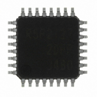
IC R8C/27 MCU FLASH 32LQFP
Manufacturer
Renesas Electronics America
Series
R8C/2x/27r
Datasheet
1.R5F21272SDFPU0.pdf
(487 pages)
Specifications of R5F21272SDFP#U0
Core Processor
R8C
Core Size
16/32-Bit
Speed
20MHz
Connectivity
I²C, LIN, SIO, SSU, UART/USART
Peripherals
LED, POR, Voltage Detect, WDT
Number Of I /o
25
Program Memory Size
8KB (8K x 8)
Program Memory Type
FLASH
Ram Size
512 x 8
Voltage - Supply (vcc/vdd)
2.2 V ~ 5.5 V
Data Converters
A/D 12x10b
Oscillator Type
Internal
Operating Temperature
-40°C ~ 85°C
Package / Case
32-LQFP
For Use With
R0K521276S000BE - KIT DEV RSK-R8C/26-29R0E521000EPB00 - PROBE EMULATOR FOR PC7501
Lead Free Status / RoHS Status
Lead free / RoHS Compliant
Eeprom Size
-
Available stocks
Company
Part Number
Manufacturer
Quantity
Price

Part Number:
R5F21272SDFP#U0R5F21272SDFP#V2
Manufacturer:
Renesas Electronics America
Quantity:
10 000


R8C/26 Group, R8C/27 Group
Rev.2.10
REJ09B0278-0210
Figure 16.26
IIC bus Mode Register
b7 b6 b5 b4 b3 b2 b1 b0
NOTES:
1.
2.
3.
4.
5.
6.
0
Rew rite betw een transfer frames. When w riting values other than 000b, w rite w hen the SCL signal is “L”.
When w riting to bits BC0 to BC2, w rite 0 to the BCWP bit using the MOV instruction.
After data including the acknow ledge bit is transferred, these bits are automatically set to 000b. When the start
condition is detected, these bits are automatically set to 000b.
Do not rew rite w hen the clock synchronous serial format is used.
The setting value is enabled in master mode of the I
bus format or w hen the clock synchronous serial format is used.
Set to 0 w hen the I
Sep 26, 2008
ICMR Register
Bit Symbol
Symbol
BCWP
WAIT
2
ICMR
BC0
BC1
BC2
(b4)
(b5)
MLS
C bus format is used.
Page 295 of 453
—
—
Bits counter 2 to 0
BC w rite protect bit
Nothing is assigned. If necessary, set to 0.
When read, the content is 1.
Reserved bit
Wait insertion bit
MSB-first/LSB-first select
bit
Address
Bit Name
00BAh
(5)
2
C bus format. It is disabled in slave mode of the I
I
read out and data bit count of next transfer w hen
w ritten).
Clock synchronous serial format (w hen read, the
remaining transfer bit count and w hen w ritten
000b).
When rew riting bits BC0 to BC2, w rite 0
simultaneously.
When read, the content is 1.
Set to 0.
0 : No w ait
1 : Wait
0 : Data transfer w ith MSB-first
1 : Data transfer w ith LSB-first
2
b2 b1 b0
b2 b1 b0
0 0 0 : 9 bits
0 0 1 : 2 bits
0 1 0 : 3 bits
0 1 1 : 4 bits
1 0 0 : 5 bits
1 0 1 : 6 bits
1 1 0 : 7 bits
1 1 1 : 8 bits
0 0 0 : 8 bits
0 0 1 : 1 bit
0 1 0 : 2 bits
0 1 1 : 3 bits
1 0 0 : 4 bits
1 0 1 : 5 bits
1 1 0 : 6 bits
1 1 1 : 7 bits
C bus format (remaining transfer bit count w hen
(Transfer data and acknow ledge bit
consecutively)
(After the clock falls for the final
data bit, “L” period is extended for tw o
transfer clocks cycles)
(1,2)
(3)
(2,4)
16. Clock Synchronous Serial Interface
After Reset
00011000b
Function
(6)
2
C
RW
RW
RW
RW
RW
RW
RW
RW
—
Related parts for R5F21272SDFP#U0
Image
Part Number
Description
Manufacturer
Datasheet
Request
R

Part Number:
Description:
KIT STARTER FOR M16C/29
Manufacturer:
Renesas Electronics America
Datasheet:

Part Number:
Description:
KIT STARTER FOR R8C/2D
Manufacturer:
Renesas Electronics America
Datasheet:

Part Number:
Description:
R0K33062P STARTER KIT
Manufacturer:
Renesas Electronics America
Datasheet:

Part Number:
Description:
KIT STARTER FOR R8C/23 E8A
Manufacturer:
Renesas Electronics America
Datasheet:

Part Number:
Description:
KIT STARTER FOR R8C/25
Manufacturer:
Renesas Electronics America
Datasheet:

Part Number:
Description:
KIT STARTER H8S2456 SHARPE DSPLY
Manufacturer:
Renesas Electronics America
Datasheet:

Part Number:
Description:
KIT STARTER FOR R8C38C
Manufacturer:
Renesas Electronics America
Datasheet:

Part Number:
Description:
KIT STARTER FOR R8C35C
Manufacturer:
Renesas Electronics America
Datasheet:

Part Number:
Description:
KIT STARTER FOR R8CL3AC+LCD APPS
Manufacturer:
Renesas Electronics America
Datasheet:
Part Number:
Description:
KIT STARTER FOR RX610
Manufacturer:
Renesas Electronics America
Datasheet:

Part Number:
Description:
KIT STARTER FOR R32C/118
Manufacturer:
Renesas Electronics America
Datasheet:

Part Number:
Description:
KIT DEV RSK-R8C/26-29
Manufacturer:
Renesas Electronics America
Datasheet:

Part Number:
Description:
KIT STARTER FOR SH7124
Manufacturer:
Renesas Electronics America
Datasheet:

Part Number:
Description:
KIT STARTER FOR H8SX/1622
Manufacturer:
Renesas Electronics America
Datasheet:

Part Number:
Description:
KIT DEV FOR SH7203
Manufacturer:
Renesas Electronics America
Datasheet: