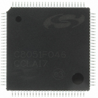
C8051F046-GQ Silicon Laboratories Inc, C8051F046-GQ Datasheet - Page 29

C8051F046-GQ
Manufacturer Part Number
C8051F046-GQ
Description
IC 8051 MCU 32K FLASH 100TQFP
Manufacturer
Silicon Laboratories Inc
Series
C8051F04xr
Specifications of C8051F046-GQ
Core Processor
8051
Core Size
8-Bit
Speed
25MHz
Connectivity
CAN, EBI/EMI, SMBus (2-Wire/I²C), SPI, UART/USART
Peripherals
Brown-out Detect/Reset, POR, PWM, Temp Sensor, WDT
Number Of I /o
64
Program Memory Size
32KB (32K x 8)
Program Memory Type
FLASH
Ram Size
4.25K x 8
Voltage - Supply (vcc/vdd)
2.7 V ~ 3.6 V
Data Converters
A/D 13x10b
Oscillator Type
Internal
Operating Temperature
-40°C ~ 85°C
Package / Case
100-TQFP, 100-VQFP
Processor Series
C8051F0x
Core
8051
Data Bus Width
8 bit
Data Ram Size
4.25 KB
Interface Type
CAN, SMBus, SPI, UART
Maximum Clock Frequency
25 MHz
Number Of Programmable I/os
64
Number Of Timers
5
Operating Supply Voltage
2.7 V to 3.6 V
Maximum Operating Temperature
+ 85 C
Mounting Style
SMD/SMT
3rd Party Development Tools
PK51, CA51, A51, ULINK2
Development Tools By Supplier
C8051F040DK
Minimum Operating Temperature
- 40 C
On-chip Adc
10 bit, 13 Channel
On-chip Dac
12 bit, 2 Channel
Package
100TQFP
Device Core
8051
Family Name
C8051F04x
Maximum Speed
25 MHz
Lead Free Status / RoHS Status
Lead free / RoHS Compliant
Eeprom Size
-
Lead Free Status / Rohs Status
Details
Other names
336-1211
Available stocks
Company
Part Number
Manufacturer
Quantity
Price
Company:
Part Number:
C8051F046-GQ
Manufacturer:
Silicon Laboratories Inc
Quantity:
10 000
Company:
Part Number:
C8051F046-GQR
Manufacturer:
AMAZING
Quantity:
67 000
Company:
Part Number:
C8051F046-GQR
Manufacturer:
Silicon Laboratories Inc
Quantity:
10 000
- Current page: 29 of 328
- Download datasheet (3Mb)
1.4.
The standard 8051 Ports (0, 1, 2, and 3) are available on the MCUs. The C8051F040/2/4/6 have 4 addi-
tional 8-bit ports (4, 5, 6, and 7) for a total of 64 general-purpose I/O Ports. The Ports behave like the stan-
dard 8051 with a few enhancements.
Each port pin can be configured as either a push-pull or open-drain output. Also, the "weak pullups" which
are normally fixed on an 8051 can be globally disabled, providing additional power saving capabilities for
low-power applications.
Perhaps the most unique enhancement is the Digital Crossbar. This is essentially a large digital switching
network that allows mapping of internal digital system resources to Port I/O pins on P0, P1, P2, and P3
(See Figure 1.9). Unlike microcontrollers with standard multiplexed digital I/O ports, all combinations of
functions are supported with all package options offered.
The on-chip counter/timers, serial buses, HW interrupts, ADC Start of Conversion input, comparator out-
puts, and other digital signals in the controller can be configured to appear on the Port I/O pins specified in
the Crossbar Control registers. This allows the user to select the exact mix of general purpose Port I/O and
digital resources needed for the particular application.
Highest
Priority
Lowest
Priority
Latches
Port
Programmable Digital I/O and Crossbar
/SYSCLK
CNVSTR0
CNVSTR2
T2, T2EX,
T3, T3EX,
T4,T4EX,
Comptr.
Outputs
UART0
UART1
SMBus
T0, T1,
/INT0,
/INT1
PCA
P0
P1
P2
P3
SPI
(P0.0-P0.7)
(P1.0-P1.7)
(P2.0-P2.7)
(P3.0-P3.7)
8
8
8
8
2
4
2
2
6
2
8
Figure 1.9. Digital Crossbar Diagram
XBR0, XBR1, XBR2,
P2MDIN, P3MDIN
XBR3 P1MDIN,
Crossbar
Rev. 1.5
To External
Registers
Decoder
Priority
Digital
Interface
Memory
(EMIF)
C8051F040/1/2/3/4/5/6/7
8
8
8
8
P0MDOUT, P1MDOUT,
P2MDOUT, P3MDOUT
Comparators
Registers
ADC2
ADC0
Input
Input
Cells
Cells
Cells
Cells
To
To
To
I/O
I/O
I/O
I/O
P0
P1
P2
P3
External
Pins
P0.0
P0.7
P1.0
P1.7
P2.0
P2.7
P3.0
P3.7
Highest
Priority
Lowest
Priority
29
Related parts for C8051F046-GQ
Image
Part Number
Description
Manufacturer
Datasheet
Request
R
Part Number:
Description:
SMD/C°/SINGLE-ENDED OUTPUT SILICON OSCILLATOR
Manufacturer:
Silicon Laboratories Inc
Part Number:
Description:
Manufacturer:
Silicon Laboratories Inc
Datasheet:
Part Number:
Description:
N/A N/A/SI4010 AES KEYFOB DEMO WITH LCD RX
Manufacturer:
Silicon Laboratories Inc
Datasheet:
Part Number:
Description:
N/A N/A/SI4010 SIMPLIFIED KEY FOB DEMO WITH LED RX
Manufacturer:
Silicon Laboratories Inc
Datasheet:
Part Number:
Description:
N/A/-40 TO 85 OC/EZLINK MODULE; F930/4432 HIGH BAND (REV E/B1)
Manufacturer:
Silicon Laboratories Inc
Part Number:
Description:
EZLink Module; F930/4432 Low Band (rev e/B1)
Manufacturer:
Silicon Laboratories Inc
Part Number:
Description:
I°/4460 10 DBM RADIO TEST CARD 434 MHZ
Manufacturer:
Silicon Laboratories Inc
Part Number:
Description:
I°/4461 14 DBM RADIO TEST CARD 868 MHZ
Manufacturer:
Silicon Laboratories Inc
Part Number:
Description:
I°/4463 20 DBM RFSWITCH RADIO TEST CARD 460 MHZ
Manufacturer:
Silicon Laboratories Inc
Part Number:
Description:
I°/4463 20 DBM RADIO TEST CARD 868 MHZ
Manufacturer:
Silicon Laboratories Inc
Part Number:
Description:
I°/4463 27 DBM RADIO TEST CARD 868 MHZ
Manufacturer:
Silicon Laboratories Inc
Part Number:
Description:
I°/4463 SKYWORKS 30 DBM RADIO TEST CARD 915 MHZ
Manufacturer:
Silicon Laboratories Inc
Part Number:
Description:
N/A N/A/-40 TO 85 OC/4463 RFMD 30 DBM RADIO TEST CARD 915 MHZ
Manufacturer:
Silicon Laboratories Inc
Part Number:
Description:
I°/4463 20 DBM RADIO TEST CARD 169 MHZ
Manufacturer:
Silicon Laboratories Inc


