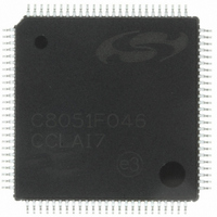
C8051F046-GQ Silicon Laboratories Inc, C8051F046-GQ Datasheet - Page 302

C8051F046-GQ
Manufacturer Part Number
C8051F046-GQ
Description
IC 8051 MCU 32K FLASH 100TQFP
Manufacturer
Silicon Laboratories Inc
Series
C8051F04xr
Specifications of C8051F046-GQ
Core Processor
8051
Core Size
8-Bit
Speed
25MHz
Connectivity
CAN, EBI/EMI, SMBus (2-Wire/I²C), SPI, UART/USART
Peripherals
Brown-out Detect/Reset, POR, PWM, Temp Sensor, WDT
Number Of I /o
64
Program Memory Size
32KB (32K x 8)
Program Memory Type
FLASH
Ram Size
4.25K x 8
Voltage - Supply (vcc/vdd)
2.7 V ~ 3.6 V
Data Converters
A/D 13x10b
Oscillator Type
Internal
Operating Temperature
-40°C ~ 85°C
Package / Case
100-TQFP, 100-VQFP
Processor Series
C8051F0x
Core
8051
Data Bus Width
8 bit
Data Ram Size
4.25 KB
Interface Type
CAN, SMBus, SPI, UART
Maximum Clock Frequency
25 MHz
Number Of Programmable I/os
64
Number Of Timers
5
Operating Supply Voltage
2.7 V to 3.6 V
Maximum Operating Temperature
+ 85 C
Mounting Style
SMD/SMT
3rd Party Development Tools
PK51, CA51, A51, ULINK2
Development Tools By Supplier
C8051F040DK
Minimum Operating Temperature
- 40 C
On-chip Adc
10 bit, 13 Channel
On-chip Dac
12 bit, 2 Channel
Package
100TQFP
Device Core
8051
Family Name
C8051F04x
Maximum Speed
25 MHz
Lead Free Status / RoHS Status
Lead free / RoHS Compliant
Eeprom Size
-
Lead Free Status / Rohs Status
Details
Other names
336-1211
Available stocks
Company
Part Number
Manufacturer
Quantity
Price
Company:
Part Number:
C8051F046-GQ
Manufacturer:
Silicon Laboratories Inc
Quantity:
10 000
Company:
Part Number:
C8051F046-GQR
Manufacturer:
AMAZING
Quantity:
67 000
Company:
Part Number:
C8051F046-GQR
Manufacturer:
Silicon Laboratories Inc
Quantity:
10 000
- Current page: 302 of 328
- Download datasheet (3Mb)
C8051F040/1/2/3/4/5/6/7
300
Bit7-5:
Bit4-3:
Bit2:
Bit1:
Bit0:
SFR Address: TMR2CF:0xC9;TMR3CF:0xC9;TMR4CF:0xC9
SFR Page TMR2CF: page 0;TMR3CF: page 1;TMR4CF: page 2
Bit7
-
Reserved.
TnM1 and TnM0: Timer Clock Mode Select Bits.
Bits used to select the Timer clock source. The sources can be the System Clock
(SYSCLK), SYSCLK divided by 2 or 12, or an external clock signal routed to Tn (port pin)
divided by 8. Clock source is selected as follows:
00: SYSCLK/12
01: SYSCLK
10: EXTERNAL CLOCK/8
11: SYSCLK/2
TOGn: Toggle output state bit.
When timer is used to toggle a port pin, this bit can be used to read the state of the output, or
can be written to in order to force the state of the output.
TnOE: Timer output enable bit.
This bit enables the timer to output a 50% duty cycle output to the timer’s assigned external
port pin.
NOTE: A timer is configured for Square Wave Output as follows:
CP/RLn = 0
C/Tn
TnOE = 1
Load RCAPnH:RCAPnL (See
page
Configure Port Pin for output (See
0: Output of toggle mode not available at Timers’ assigned port pin.
1: Output of toggle mode available at Timers’ assigned port pin.
DCEN: Decrement Enable Bit.
This bit enables the timer to count up or down as determined by the state of TnEX.
0: Timer will count up, regardless of the state of TnEX.
1: Timer will count up or down depending on the state of TnEX as follows:
Bit6
298).
-
SFR Definition 23.9. TMRnCF: Timer n Configuration
= 0
if TnEX = 0, the timer counts DOWN
if TnEX = 1, the timer counts UP.
Bit5
-
TnM1
R/W
Bit4
Section “Equation 23.1. Square Wave Frequency” on
Section “17. Port Input/Output” on page
Rev. 1.5
TnM0
R/W
Bit3
TOGn
R/W
Bit2
TnOE
R/W
Bit1
DCEN
R/W
Bit0
203).
00000000
Addressable
Reset Value
Bit
Related parts for C8051F046-GQ
Image
Part Number
Description
Manufacturer
Datasheet
Request
R
Part Number:
Description:
SMD/C°/SINGLE-ENDED OUTPUT SILICON OSCILLATOR
Manufacturer:
Silicon Laboratories Inc
Part Number:
Description:
Manufacturer:
Silicon Laboratories Inc
Datasheet:
Part Number:
Description:
N/A N/A/SI4010 AES KEYFOB DEMO WITH LCD RX
Manufacturer:
Silicon Laboratories Inc
Datasheet:
Part Number:
Description:
N/A N/A/SI4010 SIMPLIFIED KEY FOB DEMO WITH LED RX
Manufacturer:
Silicon Laboratories Inc
Datasheet:
Part Number:
Description:
N/A/-40 TO 85 OC/EZLINK MODULE; F930/4432 HIGH BAND (REV E/B1)
Manufacturer:
Silicon Laboratories Inc
Part Number:
Description:
EZLink Module; F930/4432 Low Band (rev e/B1)
Manufacturer:
Silicon Laboratories Inc
Part Number:
Description:
I°/4460 10 DBM RADIO TEST CARD 434 MHZ
Manufacturer:
Silicon Laboratories Inc
Part Number:
Description:
I°/4461 14 DBM RADIO TEST CARD 868 MHZ
Manufacturer:
Silicon Laboratories Inc
Part Number:
Description:
I°/4463 20 DBM RFSWITCH RADIO TEST CARD 460 MHZ
Manufacturer:
Silicon Laboratories Inc
Part Number:
Description:
I°/4463 20 DBM RADIO TEST CARD 868 MHZ
Manufacturer:
Silicon Laboratories Inc
Part Number:
Description:
I°/4463 27 DBM RADIO TEST CARD 868 MHZ
Manufacturer:
Silicon Laboratories Inc
Part Number:
Description:
I°/4463 SKYWORKS 30 DBM RADIO TEST CARD 915 MHZ
Manufacturer:
Silicon Laboratories Inc
Part Number:
Description:
N/A N/A/-40 TO 85 OC/4463 RFMD 30 DBM RADIO TEST CARD 915 MHZ
Manufacturer:
Silicon Laboratories Inc
Part Number:
Description:
I°/4463 20 DBM RADIO TEST CARD 169 MHZ
Manufacturer:
Silicon Laboratories Inc


