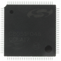
C8051F046-GQ Silicon Laboratories Inc, C8051F046-GQ Datasheet - Page 319

C8051F046-GQ
Manufacturer Part Number
C8051F046-GQ
Description
IC 8051 MCU 32K FLASH 100TQFP
Manufacturer
Silicon Laboratories Inc
Series
C8051F04xr
Specifications of C8051F046-GQ
Core Processor
8051
Core Size
8-Bit
Speed
25MHz
Connectivity
CAN, EBI/EMI, SMBus (2-Wire/I²C), SPI, UART/USART
Peripherals
Brown-out Detect/Reset, POR, PWM, Temp Sensor, WDT
Number Of I /o
64
Program Memory Size
32KB (32K x 8)
Program Memory Type
FLASH
Ram Size
4.25K x 8
Voltage - Supply (vcc/vdd)
2.7 V ~ 3.6 V
Data Converters
A/D 13x10b
Oscillator Type
Internal
Operating Temperature
-40°C ~ 85°C
Package / Case
100-TQFP, 100-VQFP
Processor Series
C8051F0x
Core
8051
Data Bus Width
8 bit
Data Ram Size
4.25 KB
Interface Type
CAN, SMBus, SPI, UART
Maximum Clock Frequency
25 MHz
Number Of Programmable I/os
64
Number Of Timers
5
Operating Supply Voltage
2.7 V to 3.6 V
Maximum Operating Temperature
+ 85 C
Mounting Style
SMD/SMT
3rd Party Development Tools
PK51, CA51, A51, ULINK2
Development Tools By Supplier
C8051F040DK
Minimum Operating Temperature
- 40 C
On-chip Adc
10 bit, 13 Channel
On-chip Dac
12 bit, 2 Channel
Package
100TQFP
Device Core
8051
Family Name
C8051F04x
Maximum Speed
25 MHz
Lead Free Status / RoHS Status
Lead free / RoHS Compliant
Eeprom Size
-
Lead Free Status / Rohs Status
Details
Other names
336-1211
Available stocks
Company
Part Number
Manufacturer
Quantity
Price
Company:
Part Number:
C8051F046-GQ
Manufacturer:
Silicon Laboratories Inc
Quantity:
10 000
Company:
Part Number:
C8051F046-GQR
Manufacturer:
AMAZING
Quantity:
67 000
Company:
Part Number:
C8051F046-GQR
Manufacturer:
Silicon Laboratories Inc
Quantity:
10 000
- Current page: 319 of 328
- Download datasheet (3Mb)
25. JTAG (IEEE 1149.1)
Each MCU has an on-chip JTAG interface and logic to support boundary scan for production and in-sys-
tem testing, Flash read/write operations, and non-intrusive in-circuit debug. The JTAG interface is fully
compliant with the IEEE 1149.1 specification. Refer to this specification for detailed descriptions of the Test
Interface and Boundary-Scan Architecture. Access of the JTAG Instruction Register (IR) and Data Regis-
ters (DR) are as described in the Test Access Port and Operation of the IEEE 1149.1 specification.
The JTAG interface is accessed via four dedicated pins on the MCU: TCK, TMS, TDI, and TDO.
Through the 16-bit JTAG Instruction Register (IR), any of the seven instructions shown in Figure 25.1 can
be commanded. There are three DRs associated with JTAG Boundary-Scan, and four associated with
Flash read/write operations on the MCU.
0xFFFF
0x0000
0x0002
0x0004
0x0082
0x0083
0x0084 Flash Address Selects FLASHADR Register which holds the address of all Flash read,
Value
Bit15
IR
Flash Control
JTAG Register Definition 25.1. IR: JTAG Instruction Register
Instruction
Flash Data
PRELOAD
SAMPLE/
EXTEST
IDCODE
BYPASS
Selects the Boundary Data Register for observability and presetting the
Selects the Boundary Data Register for control and observability of all
device pins
scan-path latches
Selects device ID Register (DEVICEID)
Selects Bypass Data Register
Selects FLASHCON Register to control how the interface logic responds
to reads and writes to the FLASHDAT Register
Selects FLASHDAT Register for reads and writes to the Flash memory
write, and erase operations
Rev. 1.5
C8051F040/1/2/3/4/5/6/7
Description
Bit0
Reset Value
0x0000
317
Related parts for C8051F046-GQ
Image
Part Number
Description
Manufacturer
Datasheet
Request
R
Part Number:
Description:
SMD/C°/SINGLE-ENDED OUTPUT SILICON OSCILLATOR
Manufacturer:
Silicon Laboratories Inc
Part Number:
Description:
Manufacturer:
Silicon Laboratories Inc
Datasheet:
Part Number:
Description:
N/A N/A/SI4010 AES KEYFOB DEMO WITH LCD RX
Manufacturer:
Silicon Laboratories Inc
Datasheet:
Part Number:
Description:
N/A N/A/SI4010 SIMPLIFIED KEY FOB DEMO WITH LED RX
Manufacturer:
Silicon Laboratories Inc
Datasheet:
Part Number:
Description:
N/A/-40 TO 85 OC/EZLINK MODULE; F930/4432 HIGH BAND (REV E/B1)
Manufacturer:
Silicon Laboratories Inc
Part Number:
Description:
EZLink Module; F930/4432 Low Band (rev e/B1)
Manufacturer:
Silicon Laboratories Inc
Part Number:
Description:
I°/4460 10 DBM RADIO TEST CARD 434 MHZ
Manufacturer:
Silicon Laboratories Inc
Part Number:
Description:
I°/4461 14 DBM RADIO TEST CARD 868 MHZ
Manufacturer:
Silicon Laboratories Inc
Part Number:
Description:
I°/4463 20 DBM RFSWITCH RADIO TEST CARD 460 MHZ
Manufacturer:
Silicon Laboratories Inc
Part Number:
Description:
I°/4463 20 DBM RADIO TEST CARD 868 MHZ
Manufacturer:
Silicon Laboratories Inc
Part Number:
Description:
I°/4463 27 DBM RADIO TEST CARD 868 MHZ
Manufacturer:
Silicon Laboratories Inc
Part Number:
Description:
I°/4463 SKYWORKS 30 DBM RADIO TEST CARD 915 MHZ
Manufacturer:
Silicon Laboratories Inc
Part Number:
Description:
N/A N/A/-40 TO 85 OC/4463 RFMD 30 DBM RADIO TEST CARD 915 MHZ
Manufacturer:
Silicon Laboratories Inc
Part Number:
Description:
I°/4463 20 DBM RADIO TEST CARD 169 MHZ
Manufacturer:
Silicon Laboratories Inc


