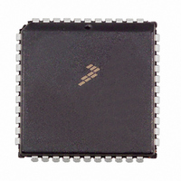
MC68HC711D3VFNE2 Freescale Semiconductor, MC68HC711D3VFNE2 Datasheet - Page 43

MC68HC711D3VFNE2
Manufacturer Part Number
MC68HC711D3VFNE2
Description
IC MCU 8BIT 4K FLASH 44-PLCC
Manufacturer
Freescale Semiconductor
Series
HC11r
Specifications of MC68HC711D3VFNE2
Core Processor
HC11
Core Size
8-Bit
Speed
2MHz
Connectivity
SCI, SPI
Peripherals
POR, WDT
Number Of I /o
26
Program Memory Size
4KB (4K x 8)
Program Memory Type
OTP
Ram Size
192 x 8
Voltage - Supply (vcc/vdd)
4.5 V ~ 5.5 V
Oscillator Type
Internal
Operating Temperature
-40°C ~ 105°C
Package / Case
44-PLCC
Lead Free Status / RoHS Status
Lead free / RoHS Compliant
Eeprom Size
-
Data Converters
-
Available stocks
Company
Part Number
Manufacturer
Quantity
Price
Company:
Part Number:
MC68HC711D3VFNE2
Manufacturer:
Freescale Semiconductor
Quantity:
10 000
INIT — RAM and I/O Mapping Register
4.2.2.2 INIT Register
RAM[3:0] — RAM Map Position
REG[3:0] — 64-Byte Register Block Position
TECHNICAL DATA
RESET:
The internal registers used to control the operation of the MCU can be relocated on 4K
boundaries within the memory space with the use of INIT. This 8-bit special-purpose
register can change the default locations of the RAM and control registers within the
MCU memory map. It can be written to only once within the first 64 E-clock cycles after
a reset, and then it becomes a read-only register.
These four bits, which specify the upper hexadecimal digit of the RAM address, control
position of RAM in the memory map. RAM can be positioned at the beginning of any
4K page in the memory map. It is initialized to address $0040 out of reset. Refer to
Table 4-3.
These four bits specify the upper hexadecimal digit of the address for the 64-byte block
of internal registers. The register block, positioned at the beginning of any 4K page in
the memory map, is initialized to address $0000 out of reset. Refer to Table 4-4.
RAM[3:0]
0000
0001
0010
0011
0100
0101
0110
0111
1000
1001
1010
1011
1100
1101
1110
1111
Table 4-3 RAM Mapping
RAM3
Bit 7
In expanded mode, ROM is located at $7000–$7FFF out of reset. In
all other modes, ROM is located at $F000–$FFFF.
0
RAM2
Freescale Semiconductor, Inc.
6
0
OPERATING MODES AND ON-CHIP MEMORY
$C040–$C0FF
$D040–$D0FF
$A040–$A0FF
$B040–$B0FF
$E040–$E0FF
$F040–$F0FF
$0040–$00FF
$1040–$10FF
$2040–$20FF
$3040–$30FF
$4040–$40FF
$5040–$50FF
$6040–$60FF
$7040–$70FF
$8040–$80FF
$9040–$90FF
For More Information On This Product,
Address
RAM1
Go to: www.freescale.com
5
0
RAM0
4
0
NOTE
REG3
Table 4-4 Register Mapping
REG[3:0]
3
0
0000
0001
0010
0011
0100
0101
0110
0111
1000
1001
1010
1011
1100
1101
1110
1111
REG2
2
0
$C000–$C03F
$D000–$D03F
$A000–$A03F
$B000–$B03F
$E000–$E03F
$F000–$F03F
$0000–$003F
$1000–$103F
$2000–$203F
$3000–$303F
$4000–$403F
$5000–$503F
$6000–$603F
$7000–$703F
$8000–$803F
$9000–$903F
REG1
Address
1
0
$003D
REG0
Bit 0
1
4-9


