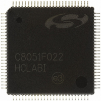
C8051F022-GQ Silicon Laboratories Inc, C8051F022-GQ Datasheet - Page 162

C8051F022-GQ
Manufacturer Part Number
C8051F022-GQ
Description
IC 8051 MCU 64K FLASH 100TQFP
Manufacturer
Silicon Laboratories Inc
Series
C8051F02xr
Specifications of C8051F022-GQ
Program Memory Type
FLASH
Program Memory Size
64KB (64K x 8)
Package / Case
100-TQFP, 100-VQFP
Core Processor
8051
Core Size
8-Bit
Speed
25MHz
Connectivity
EBI/EMI, SMBus (2-Wire/I²C), SPI, UART/USART
Peripherals
Brown-out Detect/Reset, POR, PWM, Temp Sensor, WDT
Number Of I /o
64
Ram Size
4.25K x 8
Voltage - Supply (vcc/vdd)
2.7 V ~ 3.6 V
Data Converters
A/D 8x8b, 8x10b; D/A 2x12b
Oscillator Type
Internal
Operating Temperature
-40°C ~ 85°C
Processor Series
C8051F0x
Core
8051
Data Bus Width
8 bit
Data Ram Size
4.25 KB
Interface Type
I2C/SMBus/SPI/UART
Maximum Clock Frequency
25 MHz
Number Of Programmable I/os
64
Number Of Timers
4
Operating Supply Voltage
2.7 V to 3.6 V
Maximum Operating Temperature
+ 85 C
Mounting Style
SMD/SMT
3rd Party Development Tools
PK51, CA51, A51, ULINK2
Development Tools By Supplier
C8051F020DK
Minimum Operating Temperature
- 40 C
On-chip Adc
8-ch x 8-bit or 8-ch x 10-bit
On-chip Dac
2-ch x 12-bit
No. Of I/o's
64
Ram Memory Size
4352Byte
Cpu Speed
25MHz
No. Of Timers
5
Rohs Compliant
Yes
Cpu Family
C8051F02x
Device Core
8051
Device Core Size
8b
Frequency (max)
25MHz
Total Internal Ram Size
4.25KB
# I/os (max)
64
Number Of Timers - General Purpose
5
Operating Supply Voltage (typ)
3.3V
Operating Supply Voltage (max)
3.6V
Operating Supply Voltage (min)
2.7V
Instruction Set Architecture
CISC
Operating Temp Range
-40C to 85C
Operating Temperature Classification
Industrial
Mounting
Surface Mount
Pin Count
100
Package Type
TQFP
Lead Free Status / RoHS Status
Lead free / RoHS Compliant
For Use With
336-1200 - DEV KIT FOR F020/F021/F022/F023
Eeprom Size
-
Lead Free Status / Rohs Status
Lead free / RoHS Compliant
Other names
336-1202
Available stocks
Company
Part Number
Manufacturer
Quantity
Price
Company:
Part Number:
C8051F022-GQ
Manufacturer:
Silicon Laboratories Inc
Quantity:
10 000
Part Number:
C8051F022-GQ
Manufacturer:
SILICON LABS/芯科
Quantity:
20 000
Company:
Part Number:
C8051F022-GQR
Manufacturer:
Silicon Laboratories Inc
Quantity:
10 000
C8051F020/1/2/3
The C8051F020/1/2/3 devices have a wide array of digital resources which are available through the four lower I/O
Ports: P0, P1, P2, and P3. Each of the pins on P0, P1, P2, and P3, can be defined as a General-Purpose I/O (GPIO) pin
or can be controlled by a digital peripheral or function (like UART0 or /INT1 for example), as shown in Figure 17.2.
The system designer controls which digital functions are assigned pins, limited only by the number of pins available.
This resource assignment flexibility is achieved through the use of a Priority Crossbar Decoder. Note that the state of
a Port I/O pin can always be read from its associated Data register regardless of whether that pin has been assigned to
a digital peripheral or behaves as GPIO. The Port pins on Port 1 can be used as Analog Inputs to ADC1.
An External Memory Interface which is active during the execution of a MOVX instruction whose target address
resides in off-chip memory can be active on either the lower Ports or the upper Ports. See
DATA MEMORY INTERFACE AND ON-CHIP XRAM” on page 145
Memory Interface.
The upper Ports (available on C8051F020/2) can be byte-accessed as GPIO pins.
162
Highest
Priority
Lowest
Priority
Latches
Port
T2, T2EX,
/SYSCLK
CNVSTR
T4,T4EX
Comptr.
Outputs
UART0
UART1
SMBus
T0, T1,
/INT0,
/INT1
PCA
P0
P1
P2
P3
SPI
(P0.0-P0.7)
(P1.0-P1.7)
(P2.0-P2.7)
(P3.0-P3.7)
Figure 17.2. Lower Port I/O Functional Block Diagram
8
8
8
8
2
4
2
2
6
2
8
XBR2, P1MDIN
XBR0, XBR1,
Crossbar
Decoder
To External
Registers
Priority
Rev. 1.4
Digital
Interface
Memory
(EMIF)
8
8
8
8
P0MDOUT, P1MDOUT,
P2MDOUT, P3MDOUT
Registers
for more information about the External
ADC1
Input
Cells
Cells
Cells
Cells
To
I/O
I/O
I/O
I/O
P0
P1
P2
P3
Section “16. EXTERNAL
External
Pins
P0.0
P0.7
P1.0
P1.7
P2.0
P2.7
P3.0
P3.7
Highest
Lowest
Priority
Priority


