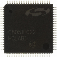
C8051F022-GQ Silicon Laboratories Inc, C8051F022-GQ Datasheet - Page 178

C8051F022-GQ
Manufacturer Part Number
C8051F022-GQ
Description
IC 8051 MCU 64K FLASH 100TQFP
Manufacturer
Silicon Laboratories Inc
Series
C8051F02xr
Specifications of C8051F022-GQ
Program Memory Type
FLASH
Program Memory Size
64KB (64K x 8)
Package / Case
100-TQFP, 100-VQFP
Core Processor
8051
Core Size
8-Bit
Speed
25MHz
Connectivity
EBI/EMI, SMBus (2-Wire/I²C), SPI, UART/USART
Peripherals
Brown-out Detect/Reset, POR, PWM, Temp Sensor, WDT
Number Of I /o
64
Ram Size
4.25K x 8
Voltage - Supply (vcc/vdd)
2.7 V ~ 3.6 V
Data Converters
A/D 8x8b, 8x10b; D/A 2x12b
Oscillator Type
Internal
Operating Temperature
-40°C ~ 85°C
Processor Series
C8051F0x
Core
8051
Data Bus Width
8 bit
Data Ram Size
4.25 KB
Interface Type
I2C/SMBus/SPI/UART
Maximum Clock Frequency
25 MHz
Number Of Programmable I/os
64
Number Of Timers
4
Operating Supply Voltage
2.7 V to 3.6 V
Maximum Operating Temperature
+ 85 C
Mounting Style
SMD/SMT
3rd Party Development Tools
PK51, CA51, A51, ULINK2
Development Tools By Supplier
C8051F020DK
Minimum Operating Temperature
- 40 C
On-chip Adc
8-ch x 8-bit or 8-ch x 10-bit
On-chip Dac
2-ch x 12-bit
No. Of I/o's
64
Ram Memory Size
4352Byte
Cpu Speed
25MHz
No. Of Timers
5
Rohs Compliant
Yes
Cpu Family
C8051F02x
Device Core
8051
Device Core Size
8b
Frequency (max)
25MHz
Total Internal Ram Size
4.25KB
# I/os (max)
64
Number Of Timers - General Purpose
5
Operating Supply Voltage (typ)
3.3V
Operating Supply Voltage (max)
3.6V
Operating Supply Voltage (min)
2.7V
Instruction Set Architecture
CISC
Operating Temp Range
-40C to 85C
Operating Temperature Classification
Industrial
Mounting
Surface Mount
Pin Count
100
Package Type
TQFP
Lead Free Status / RoHS Status
Lead free / RoHS Compliant
For Use With
336-1200 - DEV KIT FOR F020/F021/F022/F023
Eeprom Size
-
Lead Free Status / Rohs Status
Lead free / RoHS Compliant
Other names
336-1202
Available stocks
Company
Part Number
Manufacturer
Quantity
Price
Company:
Part Number:
C8051F022-GQ
Manufacturer:
Silicon Laboratories Inc
Quantity:
10 000
Part Number:
C8051F022-GQ
Manufacturer:
SILICON LABS/芯科
Quantity:
20 000
Company:
Part Number:
C8051F022-GQR
Manufacturer:
Silicon Laboratories Inc
Quantity:
10 000
C8051F020/1/2/3
Port Data register will cause the Port pin to be driven to GND, and a logic 1 will cause the Port pin to assume a high-
impedance state. The Open-Drain configuration is useful to prevent contention between devices in systems where the
Port pin participates in a shared interconnection in which multiple outputs are connected to the same physical wire.
The output modes of the Port pins on Ports 4 through 7 are determined by the bits in the P74OUT register (see
Figure 17.20). Each bit in P74OUT controls the output mode of a 4-bit bank of Port pins on Ports 4, 5, 6, and 7. A
logic 1 in P74OUT.7 will configure the output modes of 4 most-significant bits of Port 7, P7.[7:4], to Push-Pull; a
logic 0 in P74OUT.7 will configure the output modes of P7.[7:4] to Open-Drain.
17.2.3. Configuring Port Pins as Digital Inputs
A Port pin is configured as a digital input by setting its output mode to “Open-Drain” and writing a logic 1 to the
associated bit in the Port Data register. For example, P7.7 is configured as a digital input by setting P74OUT.7 to a
logic 0 and P7.7 to a logic 1.
17.2.4. Weak Pull-ups
By default, each Port pin has an internal weak pull-up device enabled which provides a resistive connection (about
100 k) between the pin and VDD. The weak pull-up devices can be globally disabled by writing a logic 1 to the
Weak Pull-up Disable bit, (WEAKPUD, XBR2.7). The weak pull-up is automatically deactivated on any pin that is
driving a logic 0; that is, an output pin will not contend with its own pull-up device.
17.2.5. External Memory Interface
If the External Memory Interface (EMIF) is enabled on the High ports (Ports 4 through 7), EMIFLE (XBR2.1) should
be set to a logic 0.
If the External Memory Interface is enabled on the High ports and an off-chip MOVX operation occurs, the External
Memory Interface will control the output states of the affected Port pins during the execution phase of the MOVX
instruction, regardless of the settings of the Port Data registers. The output configuration of the Port pins is not
affected by the EMIF operation, except that Read operations will explicitly disable the output drivers on the Data Bus
during the MOVX execution. See
Section “16. EXTERNAL DATA MEMORY INTERFACE AND ON-CHIP
XRAM” on page 145
for more information about the External Memory Interface.
178
Rev. 1.4


