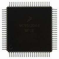
MC9S12D64MFUE Freescale Semiconductor, MC9S12D64MFUE Datasheet - Page 16

MC9S12D64MFUE
Manufacturer Part Number
MC9S12D64MFUE
Description
IC MCU 64K FLASH 25MHZ 80-QFP
Manufacturer
Freescale Semiconductor
Series
HCS12r
Datasheet
1.MC9S12A32CFUE.pdf
(128 pages)
Specifications of MC9S12D64MFUE
Core Processor
HCS12
Core Size
16-Bit
Speed
25MHz
Connectivity
CAN, I²C, SCI, SPI
Peripherals
PWM, WDT
Number Of I /o
59
Program Memory Size
64KB (64K x 8)
Program Memory Type
FLASH
Eeprom Size
1K x 8
Ram Size
4K x 8
Voltage - Supply (vcc/vdd)
2.35 V ~ 5.25 V
Data Converters
A/D 16x10b
Oscillator Type
Internal
Operating Temperature
-40°C ~ 125°C
Package / Case
80-QFP
Processor Series
S12D
Core
HCS12
Data Bus Width
16 bit
Data Ram Size
4 KB
Interface Type
CAN/I2C/SCI/SPI
Maximum Clock Frequency
25 MHz
Number Of Programmable I/os
49
Number Of Timers
8
Operating Supply Voltage
4.5 V to 5.25 V
Maximum Operating Temperature
+ 125 C
Mounting Style
SMD/SMT
3rd Party Development Tools
EWHCS12
Development Tools By Supplier
M68KIT912DP256
Minimum Operating Temperature
- 40 C
On-chip Adc
2 (8-ch x 10-bit)
Lead Free Status / RoHS Status
Lead free / RoHS Compliant
Available stocks
Company
Part Number
Manufacturer
Quantity
Price
Company:
Part Number:
MC9S12D64MFUE
Manufacturer:
Freescale Semiconductor
Quantity:
10 000
MC9S12DJ64 Device User Guide — V01.20
Document References
The Device User Guide provides information about the MC9S12DJ64 device made up of standard HCS12
blocks and the HCS12 processor core.
This document is part of the customer documentation. A complete set of device manuals also includes all
the individual Block Guides of the implemented modules. In a effort to reduce redundancy all module
specific information is located only in the respective Block Guide. If applicable, special implementation
details of the module are given in the block description sections of this document.
See Table 0-2 for names and versions of the referenced documents throughout the Device User Guide.
16
•
•
Ports
– The CAN0 pin functionality (TXCAN0, RXCAN0) is not available on port PJ7, PJ6, PM5,
– The BDLC pin functionality (TXB, RXB) is not available on port PM1 and PM0, if using a
– Do not write MODRR1 and MODRR0 Bit of Module Routing Register (PIM_9DJ64 Block
Pins not available in 80 pin QFP package
– Port H
– Port J[1:0]
– Port K
– Port M[7:6]
– Port P6
– Port S[7:4]
– PAD[15:8] (ATD1 channels)
PM4, PM3, PM2, PM1 and PM0, if using a derivative without CAN0 (see Table 0-1).
derivative without BDLC (see Table 0-1).
User Guide), if using a derivative without CAN0 (see Table 0-1).
In order to avoid floating nodes the ports should be either configured as outputs by setting the
data direction register (DDRH at Base+$0262) to $FF, or enabling the pull resistors by writing
a $FF to the pull enable register (PERH at Base+$0264).
Port J pull-up resistors are enabled out of reset on all four pins (7:6 and 1:0). Therefore care must
be taken not to disable the pull enables on PJ[1:0] by clearing the bits PERJ1 and PERJ0 at
Base+$026C.
Port K pull-up resistors are enabled out of reset, i.e. Bit 7 = PUKE = 1 in the register PUCR at
Base+$000C. Therefor care must be taken not to clear this bit.
PM7:6 must be configured as outputs or their pull resistors must be enabled to avoid floating
inputs.
PP6 must be configured as output or its pull resistor must be enabled to avoid a floating input.
PS7:4 must be configured as outputs or their pull resistors must be enabled to avoid floating
inputs.
Out of reset the ATD1 is disabled preventing current flows in the pins. Do not modify the ATD1
registers!


