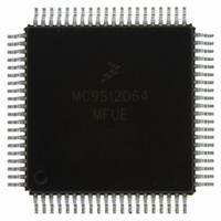
MC9S12D64MFUE Freescale Semiconductor, MC9S12D64MFUE Datasheet - Page 65

MC9S12D64MFUE
Manufacturer Part Number
MC9S12D64MFUE
Description
IC MCU 64K FLASH 25MHZ 80-QFP
Manufacturer
Freescale Semiconductor
Series
HCS12r
Datasheet
1.MC9S12A32CFUE.pdf
(128 pages)
Specifications of MC9S12D64MFUE
Core Processor
HCS12
Core Size
16-Bit
Speed
25MHz
Connectivity
CAN, I²C, SCI, SPI
Peripherals
PWM, WDT
Number Of I /o
59
Program Memory Size
64KB (64K x 8)
Program Memory Type
FLASH
Eeprom Size
1K x 8
Ram Size
4K x 8
Voltage - Supply (vcc/vdd)
2.35 V ~ 5.25 V
Data Converters
A/D 16x10b
Oscillator Type
Internal
Operating Temperature
-40°C ~ 125°C
Package / Case
80-QFP
Processor Series
S12D
Core
HCS12
Data Bus Width
16 bit
Data Ram Size
4 KB
Interface Type
CAN/I2C/SCI/SPI
Maximum Clock Frequency
25 MHz
Number Of Programmable I/os
49
Number Of Timers
8
Operating Supply Voltage
4.5 V to 5.25 V
Maximum Operating Temperature
+ 125 C
Mounting Style
SMD/SMT
3rd Party Development Tools
EWHCS12
Development Tools By Supplier
M68KIT912DP256
Minimum Operating Temperature
- 40 C
On-chip Adc
2 (8-ch x 10-bit)
Lead Free Status / RoHS Status
Lead free / RoHS Compliant
Available stocks
Company
Part Number
Manufacturer
Quantity
Price
Company:
Part Number:
MC9S12D64MFUE
Manufacturer:
Freescale Semiconductor
Quantity:
10 000
2.4.1 VDDX, VSSX — Power & Ground Pins for I/O Drivers
External power and ground for I/O drivers. Because fast signal transitions place high, short-duration
current demands on the power supply, use bypass capacitors with high-frequency characteristics and place
them as close to the MCU as possible. Bypass requirements depend on how heavily the MCU pins are
loaded.
VDDX and VSSX are the supplies for Ports J, K, M, P, T and S.
2.4.2 VDDR, VSSR — Power & Ground Pins for I/O Drivers & for Internal
Voltage Regulator
External power and ground for I/O drivers and input to the internal voltage regulator. Because fast signal
transitions place high, short-duration current demands on the power supply, use bypass capacitors with
high-frequency characteristics and place them as close to the MCU as possible. Bypass requirements
depend on how heavily the MCU pins are loaded.
VDDR and VSSR are the supplies for Ports A, B, E and H.
2.4.3 VDD1, VDD2, VSS1, VSS2 — Internal Logic Power Supply Pins
Power is supplied to the MCU through VDD and VSS. Because fast signal transitions place high,
short-duration current demands on the power supply, use bypass capacitors with high-frequency
characteristics and place them as close to the MCU as possible. This 2.5V supply is derived from the
internal voltage regulator. There is no static load on those pins allowed. The internal voltage regulator is
turned off, if VREGEN is tied to ground.
2.4.4 VDDA, VSSA — Power Supply Pins for ATD0/ATD1 and VREG
VDDA, VSSA are the power supply and ground input pins for the voltage regulator and the two analog to
digital converters. It also provides the reference for the internal voltage regulator. This allows the supply
voltage to ATD0/ATD1 and the reference voltage to be bypassed independently.
NOTE:
Mnemonic
VREGEN
VDDPLL
VSSPLL
No load allowed except for bypass capacitors.
112-pin QFP
Pin Number
43
45
97
Nominal
Voltage
2.5V
5.0V
0V
Provides operating voltage and ground for the Phased-Locked
Internal Voltage Regulator enable/disable
Loop. This allows the supply voltage to the PLL to be
bypassed independently. Internal power and ground
generated by internal regulator.
MC9S12DJ64 Device User Guide — V01.20
Description
65


