M30626FJPFP#U5C Renesas Electronics America, M30626FJPFP#U5C Datasheet - Page 45
M30626FJPFP#U5C
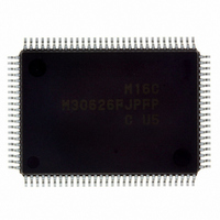
Manufacturer Part Number
M30626FJPFP#U5C
Description
IC M16C MCU FLASH 512K 100QFP
Manufacturer
Renesas Electronics America
Series
M16C™ M16C/60r
Datasheets
1.QSK-62P_PLUS.pdf
(103 pages)
2.M30622SAFPU5.pdf
(308 pages)
3.M30620SPGPU3C.pdf
(423 pages)
Specifications of M30626FJPFP#U5C
Core Processor
M16C/60
Core Size
16-Bit
Speed
24MHz
Connectivity
I²C, IEBus, UART/USART
Peripherals
DMA, WDT
Number Of I /o
85
Program Memory Size
512KB (512K x 8)
Program Memory Type
FLASH
Ram Size
31K x 8
Voltage - Supply (vcc/vdd)
2.7 V ~ 5.5 V
Data Converters
A/D 26x10b; D/A 2x8b
Oscillator Type
Internal
Operating Temperature
-20°C ~ 85°C
Package / Case
100-QFP
For Use With
867-1000 - KIT QUICK START RENESAS 62PR0K33062PS001BE - R0K33062P STARTER KITR0K33062PS000BE - KIT EVAL STARTER FOR M16C/62PM3062PT3-CPE-3 - EMULATOR COMPACT M16C/62P/30P
Lead Free Status / RoHS Status
Lead free / RoHS Compliant
Eeprom Size
-
Available stocks
Company
Part Number
Manufacturer
Quantity
Price

Part Number:
M30626FJPFP#U5CM30626FJPFP#U3C
Manufacturer:
Renesas Electronics America
Quantity:
10 000


2.4 Special Instruction Addressing
Chapter 2 Addressing Modes
dsp:20[A0]
dsp:20[A1]
[A1A0]
20-bit absolute
abs20
Address register relative with
20-bit displacement
32-bit address register indirect
The address indicated by displacement
(dsp) plus the content of address register
(A0/A1)—added not including the sign
bits—constitutes the effective address to
be operated on.
However, if the addition resulted in exceed-
ing FFFFF
ignored, and the address returns to
00000
This addressing can be used in LDE, STE,
JMPI, and JSRI instructions.
The following lists the addressing mode and
instruction combinations that can be used.
dsp:20[A0]
dsp:20[A1]
The value indicated by abs20 constitutes
the effective address to be operated on.
The effective address range is 00000
FFFFF
This addressing can be used in LDE, STE,
JSR, and JMP instructions.
The address indicated by 32 concat-
enated bits of address registers (A0
and A1) constitutes the effective
address to be operated on.
However, if the concatenated register
value exceeds FFFFF
above bit 21 are ignored.
This addressing can be used in LDE
and STE instructions.
16
16
.
.
LDE, STE, JMPI, and JSRI in-
structions
JMPI and JSRI instructions
16
, the bits above bit 21 are
16
, the bits
16
to
27
A0 / A1
LDE, STE instructions
JMPI, JSRI instructions
b31
A0
address-H
A1
abs20
Register
address
Register
address
Register
PC
2.4 Special Instruction Addressing
address
b16 b15
address-L
Memory
dsp
dsp
Memory
A0
b0
Memory
Memory
Related parts for M30626FJPFP#U5C
Image
Part Number
Description
Manufacturer
Datasheet
Request
R

Part Number:
Description:
KIT STARTER FOR M16C/29
Manufacturer:
Renesas Electronics America
Datasheet:

Part Number:
Description:
KIT STARTER FOR R8C/2D
Manufacturer:
Renesas Electronics America
Datasheet:

Part Number:
Description:
R0K33062P STARTER KIT
Manufacturer:
Renesas Electronics America
Datasheet:

Part Number:
Description:
KIT STARTER FOR R8C/23 E8A
Manufacturer:
Renesas Electronics America
Datasheet:

Part Number:
Description:
KIT STARTER FOR R8C/25
Manufacturer:
Renesas Electronics America
Datasheet:

Part Number:
Description:
KIT STARTER H8S2456 SHARPE DSPLY
Manufacturer:
Renesas Electronics America
Datasheet:

Part Number:
Description:
KIT STARTER FOR R8C38C
Manufacturer:
Renesas Electronics America
Datasheet:

Part Number:
Description:
KIT STARTER FOR R8C35C
Manufacturer:
Renesas Electronics America
Datasheet:

Part Number:
Description:
KIT STARTER FOR R8CL3AC+LCD APPS
Manufacturer:
Renesas Electronics America
Datasheet:
Part Number:
Description:
KIT STARTER FOR RX610
Manufacturer:
Renesas Electronics America
Datasheet:

Part Number:
Description:
KIT STARTER FOR R32C/118
Manufacturer:
Renesas Electronics America
Datasheet:

Part Number:
Description:
KIT DEV RSK-R8C/26-29
Manufacturer:
Renesas Electronics America
Datasheet:

Part Number:
Description:
KIT STARTER FOR SH7124
Manufacturer:
Renesas Electronics America
Datasheet:

Part Number:
Description:
KIT STARTER FOR H8SX/1622
Manufacturer:
Renesas Electronics America
Datasheet:

Part Number:
Description:
KIT DEV FOR SH7203
Manufacturer:
Renesas Electronics America
Datasheet: