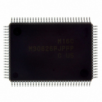
M30626FJPFP#U5C Renesas Electronics America, M30626FJPFP#U5C Datasheet - Page 185

M30626FJPFP#U5C
Manufacturer Part Number
M30626FJPFP#U5C
Description
IC M16C MCU FLASH 512K 100QFP
Manufacturer
Renesas Electronics America
Series
M16C™ M16C/60r
Datasheets
1.QSK-62P_PLUS.pdf
(103 pages)
2.M30622SAFPU5.pdf
(308 pages)
3.M30620SPGPU3C.pdf
(423 pages)
Specifications of M30626FJPFP#U5C
Core Processor
M16C/60
Core Size
16-Bit
Speed
24MHz
Connectivity
I²C, IEBus, UART/USART
Peripherals
DMA, WDT
Number Of I /o
85
Program Memory Size
512KB (512K x 8)
Program Memory Type
FLASH
Ram Size
31K x 8
Voltage - Supply (vcc/vdd)
2.7 V ~ 5.5 V
Data Converters
A/D 26x10b; D/A 2x8b
Oscillator Type
Internal
Operating Temperature
-20°C ~ 85°C
Package / Case
100-QFP
For Use With
867-1000 - KIT QUICK START RENESAS 62PR0K33062PS001BE - R0K33062P STARTER KITR0K33062PS000BE - KIT EVAL STARTER FOR M16C/62PM3062PT3-CPE-3 - EMULATOR COMPACT M16C/62P/30P
Lead Free Status / RoHS Status
Lead free / RoHS Compliant
Eeprom Size
-
Available stocks
Company
Part Number
Manufacturer
Quantity
Price
Part Number:
M30626FJPFP#U5CM30626FJPFP#U3C
Manufacturer:
Renesas Electronics America
Quantity:
10 000
- Current page: 185 of 423
- Download datasheet (5Mb)
M16C/62P Group (M16C/62P, M16C/62PT)
Rev.2.41
REJ09B0185-0241
Figure 16.3
Three-Phase Control Register 1
b7 b6 b5 b4 b3 b2 b1 b0
NOTES :
0
1.
2.
Mode
TA11, TA21 and TA41
Registers
INV00 and INV01 Bit
INV13 Bit
3.
4.
5.
Rew rite the INVC1 register after the PRC1 bit in the PRCR register is set to “1” (w rite enable).
The timers A1, A2, A4, and B2 must be stopped during rew rite.
The follow ing table lists how the INV11 bit w orks.
When the INV06 bit is set to “1” (saw tooth w ave modulation mode), set the INV11 bit to “0” (three-phase mode 0).
Also, w hen the INV11 bit is set to “0”, set the PWCON bit in the TB2SC register to “0” (Timer B2 is reloaded w hen
Timer B2 underflow s).
The INV13 bit is enabled only w hen the INV06 bit is set to “0” (Triangular w ave modulation mode) and the INV11 bit to
“1” (three-phase mode 1).
If the follow ing conditions are all met, set the INV16 bit to “1” (rising edge of the three-phase output shift register).
If above conditions are not met, set the INV16 bit to “0” (falling edge of a one-shot pulse of Timer A1, A2, A4).
Jan 10, 2006
• The INV15 bit is set to “0” (dead time timer enabled)
• The Dij bit (i=U, V or W, j=0, 1) and DiBj bit alw ays have different values w hen the INV03 bit is set to “1”.
(The positive-phase and negative-phase alw ays output opposite level signals.)
INVC1 Register
Item
Bit Symbol
Symbol
INVC1
INV10
INV11
INV12
INV13
INV14
INV15
INV16
(b7)
—
Page 168 of 390
Timer A1, A2 and A4 Start
Trigger Select Bit
Timer A1-1, A2-1 and A4-1
Control Bit
Dead Time Timer Count
Source Select Bit
Carrier Wave Detect Bit
Output Polarity Control Bit
Dead Time Disable Bit
Dead Time Timer Trigger
Select Bit
Reserved Bit
Three-phase mode 0
Not used
Disabled.
The ICTB2 counter is incremented
w henever Timer B2 underflow s
Disabled
(1)
Address
Bit Name
0349h
(2, 3)
INV11=0
(4)
0 : Timer B2 underflow
1 : Timer B2 underflow and w rite to Timer B2
0 : Three-phase mode 0
1 : Three-phase mode 1
0 : f1 or f2
1 : f1 divided-by-2 or f2 divided-by-2
0 : Timer A1 reload control signal is “0”
1 : Timer A1 reload control signal is “1”
0 : Active “L” of an output w aveform
1 : Active “H” of an output w aveform
0 : Enables dead time
1 : Disables dead time
0 : Falling edge of a one-shot pulse of Timer A1,
1 : Rising edge of the three-phase output shift
Set to “0”
A2, A4
register (U-, V-, W-phase)
16. Three-Phase Motor Control Timer Function
(5)
Three-phase mode 1
Used
Enabled
Enabled w hen INV11=1 and INV06=0
Function
After Reset
INV11=1
00h
RW
RW
RW
RW
RW
RW
RW
RW
RO
Related parts for M30626FJPFP#U5C
Image
Part Number
Description
Manufacturer
Datasheet
Request
R

Part Number:
Description:
KIT STARTER FOR M16C/29
Manufacturer:
Renesas Electronics America
Datasheet:

Part Number:
Description:
KIT STARTER FOR R8C/2D
Manufacturer:
Renesas Electronics America
Datasheet:

Part Number:
Description:
R0K33062P STARTER KIT
Manufacturer:
Renesas Electronics America
Datasheet:

Part Number:
Description:
KIT STARTER FOR R8C/23 E8A
Manufacturer:
Renesas Electronics America
Datasheet:

Part Number:
Description:
KIT STARTER FOR R8C/25
Manufacturer:
Renesas Electronics America
Datasheet:

Part Number:
Description:
KIT STARTER H8S2456 SHARPE DSPLY
Manufacturer:
Renesas Electronics America
Datasheet:

Part Number:
Description:
KIT STARTER FOR R8C38C
Manufacturer:
Renesas Electronics America
Datasheet:

Part Number:
Description:
KIT STARTER FOR R8C35C
Manufacturer:
Renesas Electronics America
Datasheet:

Part Number:
Description:
KIT STARTER FOR R8CL3AC+LCD APPS
Manufacturer:
Renesas Electronics America
Datasheet:

Part Number:
Description:
KIT STARTER FOR RX610
Manufacturer:
Renesas Electronics America
Datasheet:

Part Number:
Description:
KIT STARTER FOR R32C/118
Manufacturer:
Renesas Electronics America
Datasheet:

Part Number:
Description:
KIT DEV RSK-R8C/26-29
Manufacturer:
Renesas Electronics America
Datasheet:

Part Number:
Description:
KIT STARTER FOR SH7124
Manufacturer:
Renesas Electronics America
Datasheet:

Part Number:
Description:
KIT STARTER FOR H8SX/1622
Manufacturer:
Renesas Electronics America
Datasheet:

Part Number:
Description:
KIT DEV FOR SH7203
Manufacturer:
Renesas Electronics America
Datasheet:


