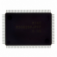
M30626FJPFP#U5C Renesas Electronics America, M30626FJPFP#U5C Datasheet - Page 201

M30626FJPFP#U5C
Manufacturer Part Number
M30626FJPFP#U5C
Description
IC M16C MCU FLASH 512K 100QFP
Manufacturer
Renesas Electronics America
Series
M16C™ M16C/60r
Datasheets
1.QSK-62P_PLUS.pdf
(103 pages)
2.M30622SAFPU5.pdf
(308 pages)
3.M30620SPGPU3C.pdf
(423 pages)
Specifications of M30626FJPFP#U5C
Core Processor
M16C/60
Core Size
16-Bit
Speed
24MHz
Connectivity
I²C, IEBus, UART/USART
Peripherals
DMA, WDT
Number Of I /o
85
Program Memory Size
512KB (512K x 8)
Program Memory Type
FLASH
Ram Size
31K x 8
Voltage - Supply (vcc/vdd)
2.7 V ~ 5.5 V
Data Converters
A/D 26x10b; D/A 2x8b
Oscillator Type
Internal
Operating Temperature
-20°C ~ 85°C
Package / Case
100-QFP
For Use With
867-1000 - KIT QUICK START RENESAS 62PR0K33062PS001BE - R0K33062P STARTER KITR0K33062PS000BE - KIT EVAL STARTER FOR M16C/62PM3062PT3-CPE-3 - EMULATOR COMPACT M16C/62P/30P
Lead Free Status / RoHS Status
Lead free / RoHS Compliant
Eeprom Size
-
Available stocks
Company
Part Number
Manufacturer
Quantity
Price
Part Number:
M30626FJPFP#U5CM30626FJPFP#U3C
Manufacturer:
Renesas Electronics America
Quantity:
10 000
- Current page: 201 of 423
- Download datasheet (5Mb)
M16C/62P Group (M16C/62P, M16C/62PT)
Rev.2.41
REJ09B0185-0241
Figure 17.8
UARTi Transmit/Receive Control Register 0 (i=0 to 2)
b7 b6 b5 b4 b3 b2 b1 b0
NOTES :
1.
2.
3.
4.
5.
6.
Set the corresponding port direction bit for each CLKi
TXD2/SDA2 and SCL2 are N-channel open-drain output. Cannot be set to the CMOS output. No NCH bit in U2C0
register is assigned. When w rite, set to “0”.
The UFORM bit is enabled w hen the SMD2 to SMD0 bits in the UiMR register are set to “001b” (clock synchronous
serial I/O mode), or “101b” (UART mode, 8-bit transfer data).
Set this bit to “1” w hen the SMD2 to SMD0 bits are set to “010b” (I
are set to “100b” (UART mode, 7-bit transfer data) or “110b” (UART mode, 9-bit transfer data).
______
CTS1
Selected by PCLK1 bit in the PCLKR register.
When changing the CLK1 to CLK0 bits, set the UiBRG register.
bit in the UCON register = 0 (CTS0
Jan 10, 2006
/RTS1
______
UiC0 Register
can be used w hen the CLKMD1 bit in the UCON register = 0 (only CLK1 output) and the RCSP
Bit Symbol
U0C0 to U2C0
UFORM
CKPOL
TXEPT
CLK0
CLK1
CRS
CRD
NCH
Page 184 of 390
Symbol
UiBRG Count Source
Select Bit
_____
CTS/
Select Bit
Transmit Register Empty
Flag
_____
CTS/
Data Output Select Bit
CLK Polarity Select Bit
Transfer Format Select
Bit
______
(3)
_____
RTS
_____
RTS
/RTS0
______
03A4h, 03ACh, 037Ch
Bit Name
Function
Disable Bit
(6)
(4)
not separated).
Address
______
(2)
pin to “0” (input mode).
b1 b0
0 0 : f1SIO or f2SIO is selected
0 1 : f8SIO is selected
1 0 : f32SIO is selected
1 1 : Do not set to this value
Effective w hen CRD = 0
0 : CTS
1 : RTS
0 : Data present in transmit register
1 : No data present in transmit register
0 : CTS/
1 : CTS
0 : TXDi/SDAi and SCLi pins are CMOS output
1 : TXDi/SDAi and SCLi pins are N-channel
0 : Transmit data is output at falling edge of transfer
1 : Transmit data is output at rising edge of transfer
0 : LSB first
1 : MSB first
(P6_0, P6_4 and P7_3 can be used as I/O ports)
_____
_____
(during transmission)
(transmission completed)
_____
____
open-drain output
clock and receive data is input at rising edge
clock and receive data is input at falling edge
/RTS
function is selected
function is selected
____
RTS
____
2
C mode), and to “0” w hen the SMD2 to SMD0 bits
function enabled
function disabled
Function
After Reset
00001000b
(1)
(5)
17. Serial Interface
RW
RW
RW
RW
RW
RW
RW
RW
RO
Related parts for M30626FJPFP#U5C
Image
Part Number
Description
Manufacturer
Datasheet
Request
R

Part Number:
Description:
KIT STARTER FOR M16C/29
Manufacturer:
Renesas Electronics America
Datasheet:

Part Number:
Description:
KIT STARTER FOR R8C/2D
Manufacturer:
Renesas Electronics America
Datasheet:

Part Number:
Description:
R0K33062P STARTER KIT
Manufacturer:
Renesas Electronics America
Datasheet:

Part Number:
Description:
KIT STARTER FOR R8C/23 E8A
Manufacturer:
Renesas Electronics America
Datasheet:

Part Number:
Description:
KIT STARTER FOR R8C/25
Manufacturer:
Renesas Electronics America
Datasheet:

Part Number:
Description:
KIT STARTER H8S2456 SHARPE DSPLY
Manufacturer:
Renesas Electronics America
Datasheet:

Part Number:
Description:
KIT STARTER FOR R8C38C
Manufacturer:
Renesas Electronics America
Datasheet:

Part Number:
Description:
KIT STARTER FOR R8C35C
Manufacturer:
Renesas Electronics America
Datasheet:

Part Number:
Description:
KIT STARTER FOR R8CL3AC+LCD APPS
Manufacturer:
Renesas Electronics America
Datasheet:

Part Number:
Description:
KIT STARTER FOR RX610
Manufacturer:
Renesas Electronics America
Datasheet:

Part Number:
Description:
KIT STARTER FOR R32C/118
Manufacturer:
Renesas Electronics America
Datasheet:

Part Number:
Description:
KIT DEV RSK-R8C/26-29
Manufacturer:
Renesas Electronics America
Datasheet:

Part Number:
Description:
KIT STARTER FOR SH7124
Manufacturer:
Renesas Electronics America
Datasheet:

Part Number:
Description:
KIT STARTER FOR H8SX/1622
Manufacturer:
Renesas Electronics America
Datasheet:

Part Number:
Description:
KIT DEV FOR SH7203
Manufacturer:
Renesas Electronics America
Datasheet:


