M30626FJPFP#U5C Renesas Electronics America, M30626FJPFP#U5C Datasheet - Page 305
M30626FJPFP#U5C
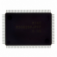
Manufacturer Part Number
M30626FJPFP#U5C
Description
IC M16C MCU FLASH 512K 100QFP
Manufacturer
Renesas Electronics America
Series
M16C™ M16C/60r
Datasheets
1.QSK-62P_PLUS.pdf
(103 pages)
2.M30622SAFPU5.pdf
(308 pages)
3.M30620SPGPU3C.pdf
(423 pages)
Specifications of M30626FJPFP#U5C
Core Processor
M16C/60
Core Size
16-Bit
Speed
24MHz
Connectivity
I²C, IEBus, UART/USART
Peripherals
DMA, WDT
Number Of I /o
85
Program Memory Size
512KB (512K x 8)
Program Memory Type
FLASH
Ram Size
31K x 8
Voltage - Supply (vcc/vdd)
2.7 V ~ 5.5 V
Data Converters
A/D 26x10b; D/A 2x8b
Oscillator Type
Internal
Operating Temperature
-20°C ~ 85°C
Package / Case
100-QFP
For Use With
867-1000 - KIT QUICK START RENESAS 62PR0K33062PS001BE - R0K33062P STARTER KITR0K33062PS000BE - KIT EVAL STARTER FOR M16C/62PM3062PT3-CPE-3 - EMULATOR COMPACT M16C/62P/30P
Lead Free Status / RoHS Status
Lead free / RoHS Compliant
Eeprom Size
-
Available stocks
Company
Part Number
Manufacturer
Quantity
Price

Part Number:
M30626FJPFP#U5CM30626FJPFP#U3C
Manufacturer:
Renesas Electronics America
Quantity:
10 000


M16C/62P Group (M16C/62P, M16C/62PT)
Rev.2.41
REJ09B0185-0241
Figure 22.11
22.3.5.5
The block erase command erases each block.
By writing “xx20h” in the first bus cycle and “xxD0h” to the highest-order even address of a block in the
second bus cycle, an auto erase operation (erase and verify) will start in the specified block.
The FMR00 bit in the FMR0 register indicates whether an auto erase operation has been completed.
The FMR00 bit is set to “0” (busy) during auto erase and to “1” (ready) when the auto erase operation is
completed.
After the completion of an auto erase operation, the FMR07 bit in the FMR0 register indicates whether or not
the auto erase operation has been completed as expected. (Refer to 22.3.8 Full Status Check.)
Figure 22.11 shows a Flow Chart of the Block Erase Command Programming.
The lock bit protects each block from being programmed inadvertently. (Refer to 22.3.6 Data Protect
Function.)
In EW1 mode, do not execute this command on the block where the rewrite control program is allocated. In
EW0 mode, the microcomputer enters read status register mode as soon as an auto erase operation starts. The
status register can be read. The SR7 bit in the status register is set to “0” at the same time an auto erase
operation starts. It is set to “1” when an auto erase operation is completed. The microcomputer remains in read
status register mode until the read array command or read lock bit status command is written. Also execute the
clear status register command and block erase command at least 3 times until an erase error is not generated
when an erase error is generated.
Jan 10, 2006
Block Erase Command
Block Erase Command
NOTES:
1. Write the command code and data to even addresses.
2. Refer to “Figure 22.14 Full Status Check and Handling Procedure
3. Execute the clear status register command and block erase
for Each Error”.
command at least 3 times until an erase error is not generated when
an erase error is generated.
Page 288 of 390
Write the command code “xx20h”
Write “xxD0h” to the highest-order
Block erase operation is
Full status check
block address
FMR00=1?
completed
Start
YES
(2, 3)
NO
(1)
22. Flash Memory Version
Related parts for M30626FJPFP#U5C
Image
Part Number
Description
Manufacturer
Datasheet
Request
R

Part Number:
Description:
KIT STARTER FOR M16C/29
Manufacturer:
Renesas Electronics America
Datasheet:

Part Number:
Description:
KIT STARTER FOR R8C/2D
Manufacturer:
Renesas Electronics America
Datasheet:

Part Number:
Description:
R0K33062P STARTER KIT
Manufacturer:
Renesas Electronics America
Datasheet:

Part Number:
Description:
KIT STARTER FOR R8C/23 E8A
Manufacturer:
Renesas Electronics America
Datasheet:

Part Number:
Description:
KIT STARTER FOR R8C/25
Manufacturer:
Renesas Electronics America
Datasheet:

Part Number:
Description:
KIT STARTER H8S2456 SHARPE DSPLY
Manufacturer:
Renesas Electronics America
Datasheet:

Part Number:
Description:
KIT STARTER FOR R8C38C
Manufacturer:
Renesas Electronics America
Datasheet:

Part Number:
Description:
KIT STARTER FOR R8C35C
Manufacturer:
Renesas Electronics America
Datasheet:

Part Number:
Description:
KIT STARTER FOR R8CL3AC+LCD APPS
Manufacturer:
Renesas Electronics America
Datasheet:
Part Number:
Description:
KIT STARTER FOR RX610
Manufacturer:
Renesas Electronics America
Datasheet:

Part Number:
Description:
KIT STARTER FOR R32C/118
Manufacturer:
Renesas Electronics America
Datasheet:

Part Number:
Description:
KIT DEV RSK-R8C/26-29
Manufacturer:
Renesas Electronics America
Datasheet:

Part Number:
Description:
KIT STARTER FOR SH7124
Manufacturer:
Renesas Electronics America
Datasheet:

Part Number:
Description:
KIT STARTER FOR H8SX/1622
Manufacturer:
Renesas Electronics America
Datasheet:

Part Number:
Description:
KIT DEV FOR SH7203
Manufacturer:
Renesas Electronics America
Datasheet: