M30626FJPFP#U5C Renesas Electronics America, M30626FJPFP#U5C Datasheet - Page 59
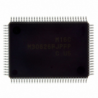
M30626FJPFP#U5C
Manufacturer Part Number
M30626FJPFP#U5C
Description
IC M16C MCU FLASH 512K 100QFP
Manufacturer
Renesas Electronics America
Series
M16C™ M16C/60r
Datasheets
1.QSK-62P_PLUS.pdf
(103 pages)
2.M30622SAFPU5.pdf
(308 pages)
3.M30620SPGPU3C.pdf
(423 pages)
Specifications of M30626FJPFP#U5C
Core Processor
M16C/60
Core Size
16-Bit
Speed
24MHz
Connectivity
I²C, IEBus, UART/USART
Peripherals
DMA, WDT
Number Of I /o
85
Program Memory Size
512KB (512K x 8)
Program Memory Type
FLASH
Ram Size
31K x 8
Voltage - Supply (vcc/vdd)
2.7 V ~ 5.5 V
Data Converters
A/D 26x10b; D/A 2x8b
Oscillator Type
Internal
Operating Temperature
-20°C ~ 85°C
Package / Case
100-QFP
For Use With
867-1000 - KIT QUICK START RENESAS 62PR0K33062PS001BE - R0K33062P STARTER KITR0K33062PS000BE - KIT EVAL STARTER FOR M16C/62PM3062PT3-CPE-3 - EMULATOR COMPACT M16C/62P/30P
Lead Free Status / RoHS Status
Lead free / RoHS Compliant
Eeprom Size
-
Available stocks
Company
Part Number
Manufacturer
Quantity
Price

Part Number:
M30626FJPFP#U5CM30626FJPFP#U3C
Manufacturer:
Renesas Electronics America
Quantity:
10 000


M16C/62P Group (M16C/62P, M16C/62PT)
Rev.2.41
REJ09B0185-0241
5.2
Table 5.1
NOTES:
P0
P1
P2, P3, P4_0 to P4_3
P4_4
P4_5 to P4_7
P5_0
P5_1
P5_2
P5_3
P5_4
P5_5
P5_6
P5_7
P6, P7, P8_0 to P8_4,
P8_6, P8_7, P9, P10
P11, P12, P13, P14_0,
P14_1
1. Shown here is the valid pin state when the internal power supply voltage has stabilized after power
2. P11, P12, P13, P14_0, P14_1 pins exist in 128-pin version.
The microcomputer resets pins, the CPU or SFR by setting the built-in voltage detect circuit. The voltage detect
circuit monitors the voltage applied to the VCC1 pin.
When the VC26 bit in the VCR2 register is set to “1” (reset level detect circuit enabled), the microcomputer
resets pins, the CPU and SFR as soon as the voltage that is applied to the VCC1 pin drops to Vdet3 or below.
The microcomputer resets pins and it is in a reset state when the voltage that is applied to the VCC1 pin is
Vdet3 or below. The microcomputer resets pins, CPU and SFR with Vdet3r or above and it executes the
program from the address determined by the reset vector. The microcomputer executes the program after
detecting Vdet3r and waiting td(S-R) ms. The same pins and registers are reset by the hardware reset 1 and
brown-out detection reset (hardware reset 2), and are also placed in the same reset state.
The microcomputer cannot exit stop mode by the brown-out detection reset (hardware reset 2).
on.
When CNVSS = VCC1, the pin state is indeterminate until the internal power supply voltage
stabilizes.
Pin Name
Brown-out Detection Reset (Hardware Reset 2)
(2)
Jan 10, 2006
Pin Status When RESET Pin Level is “L”
Page 42 of 390
Input port
Input port
Input port
Input port
Input port
Input port
Input port
Input port
Input port
Input port
Input port
Input port
Input port
Input port
Input port
CNVSS = VSS
Data input
Data input
Address output (underfined)
CS0 output (“H” is output)
Input port (Pulled high)
WR output (“H” is output)
BHE output (undefined)
RD output (“H” is output)
BCLK output
HLDA output (The output
value
depends on the input to the
HOLD pin)
HOLD input
ALE output (“L” is output)
RDY input
Input port
Input port
BYTE = VSS
Status
CNVSS = VCC1
Data input
Input port
Address output (underfined)
CS0 output (“H” is output)
Input port (Pulled high)
WR output (“H” is output)
BHE output (undefined)
RD output (“H” is output)
BCLK output
HLDA output (The output
value
depends on the input to the
HOLD pin)
HOLD input
ALE output (“L” is output)
RDY input
Input port
Input port
(1)
BYTE = VCC1
5. Reset
Related parts for M30626FJPFP#U5C
Image
Part Number
Description
Manufacturer
Datasheet
Request
R

Part Number:
Description:
KIT STARTER FOR M16C/29
Manufacturer:
Renesas Electronics America
Datasheet:

Part Number:
Description:
KIT STARTER FOR R8C/2D
Manufacturer:
Renesas Electronics America
Datasheet:

Part Number:
Description:
R0K33062P STARTER KIT
Manufacturer:
Renesas Electronics America
Datasheet:

Part Number:
Description:
KIT STARTER FOR R8C/23 E8A
Manufacturer:
Renesas Electronics America
Datasheet:

Part Number:
Description:
KIT STARTER FOR R8C/25
Manufacturer:
Renesas Electronics America
Datasheet:

Part Number:
Description:
KIT STARTER H8S2456 SHARPE DSPLY
Manufacturer:
Renesas Electronics America
Datasheet:

Part Number:
Description:
KIT STARTER FOR R8C38C
Manufacturer:
Renesas Electronics America
Datasheet:

Part Number:
Description:
KIT STARTER FOR R8C35C
Manufacturer:
Renesas Electronics America
Datasheet:

Part Number:
Description:
KIT STARTER FOR R8CL3AC+LCD APPS
Manufacturer:
Renesas Electronics America
Datasheet:
Part Number:
Description:
KIT STARTER FOR RX610
Manufacturer:
Renesas Electronics America
Datasheet:

Part Number:
Description:
KIT STARTER FOR R32C/118
Manufacturer:
Renesas Electronics America
Datasheet:

Part Number:
Description:
KIT DEV RSK-R8C/26-29
Manufacturer:
Renesas Electronics America
Datasheet:

Part Number:
Description:
KIT STARTER FOR SH7124
Manufacturer:
Renesas Electronics America
Datasheet:

Part Number:
Description:
KIT STARTER FOR H8SX/1622
Manufacturer:
Renesas Electronics America
Datasheet:

Part Number:
Description:
KIT DEV FOR SH7203
Manufacturer:
Renesas Electronics America
Datasheet: