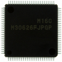
M30626FJPGP#U3C Renesas Electronics America, M30626FJPGP#U3C Datasheet - Page 113

M30626FJPGP#U3C
Manufacturer Part Number
M30626FJPGP#U3C
Description
IC M16C MCU FLASH 512K 100LQFP
Manufacturer
Renesas Electronics America
Series
M16C™ M16C/60r
Datasheets
1.QSK-62P_PLUS.pdf
(103 pages)
2.M30622SAFPU5.pdf
(308 pages)
3.M30620SPGPU3C.pdf
(423 pages)
Specifications of M30626FJPGP#U3C
Core Processor
M16C/60
Core Size
16-Bit
Speed
24MHz
Connectivity
I²C, IEBus, UART/USART
Peripherals
DMA, WDT
Number Of I /o
85
Program Memory Size
512KB (512K x 8)
Program Memory Type
FLASH
Ram Size
31K x 8
Voltage - Supply (vcc/vdd)
2.7 V ~ 5.5 V
Data Converters
A/D 26x10b; D/A 2x8b
Oscillator Type
Internal
Operating Temperature
-40°C ~ 85°C
Package / Case
100-LQFP
For Use With
867-1000 - KIT QUICK START RENESAS 62PR0K33062PS001BE - R0K33062P STARTER KITR0K33062PS000BE - KIT EVAL STARTER FOR M16C/62PM3062PT3-CPE-3 - EMULATOR COMPACT M16C/62P/30P
Lead Free Status / RoHS Status
Lead free / RoHS Compliant
Eeprom Size
-
Available stocks
Company
Part Number
Manufacturer
Quantity
Price
- Current page: 113 of 423
- Download datasheet (5Mb)
M16C/62P Group (M16C/62P, M16C/62PT)
Rev.2.41
REJ09B0185-0241
10.4.2
Table 10.4
A0 to A19, D0 to D15, CS0 to CS3,
BHE
RD, WR, WRL, WRH
HLDA, BCLK
ALE
I/O ports
CLKOUT
10.4.2.1
10.4.2.2
10.4.2.3
In wait mode, the CPU clock is turned off, so are the CPU (because operated by the CPU clock) and the
watchdog timer. However, if the PM22 bit in the PM2 register is “1” (on-chip oscillator clock for the watchdog
timer count source), the watchdog timer remains active. Because the main clock, sub clock and on-chip
oscillator clock all are on, the peripheral functions using these clocks keep operating.
If the CM02 bit in the CM0 register is “1” (peripheral function clocks turned off during wait mode), the f1, f2,
f8, f32, f1SIO, f8SIO, f32SIO and fAD clocks are turned off when in wait mode, with the power consumption
reduced that much. However, fC32 remains on.
The microcomputer is placed into wait mode by executing the WAIT instruction.
When the CM11 bit = 1 (CPU clock source is the PLL clock), be sure to clear the CM11 bit in the CM1 register
to “0” (CPU clock source is the main clock) before going to wait mode. The power consumption of the chip can
be reduced by clearing the PLC07 bit in the PLC0 register to “0” (PLL stops).
Table 10.4 lists Pin Status During Wait Mode.
Jan 10, 2006
Wait Mode
When fC selected
When f8, f32 selected
Peripheral Function Clock Stop Function
Pin Status During Wait Mode
Entering Wait Mode
Pin Status During Wait Mode
Pin
Page 96 of 390
Retains status before wait mode Does not become a bus control
“H”
“H”
“L”
Retains status before wait mode Retains status before wait mode
Does not become a CLKOUT pin Does not stop
Memory Expansion Mode
Microprocessor Mode
pin
Does not stop when the CM02 bit
is “0”.
When the CM02 bit is “1”, the
status immediately prior to
entering wait mode is
maintained.
Single-Chip Mode
10. Clock Generation Circuit
Related parts for M30626FJPGP#U3C
Image
Part Number
Description
Manufacturer
Datasheet
Request
R

Part Number:
Description:
KIT STARTER FOR M16C/29
Manufacturer:
Renesas Electronics America
Datasheet:

Part Number:
Description:
KIT STARTER FOR R8C/2D
Manufacturer:
Renesas Electronics America
Datasheet:

Part Number:
Description:
R0K33062P STARTER KIT
Manufacturer:
Renesas Electronics America
Datasheet:

Part Number:
Description:
KIT STARTER FOR R8C/23 E8A
Manufacturer:
Renesas Electronics America
Datasheet:

Part Number:
Description:
KIT STARTER FOR R8C/25
Manufacturer:
Renesas Electronics America
Datasheet:

Part Number:
Description:
KIT STARTER H8S2456 SHARPE DSPLY
Manufacturer:
Renesas Electronics America
Datasheet:

Part Number:
Description:
KIT STARTER FOR R8C38C
Manufacturer:
Renesas Electronics America
Datasheet:

Part Number:
Description:
KIT STARTER FOR R8C35C
Manufacturer:
Renesas Electronics America
Datasheet:

Part Number:
Description:
KIT STARTER FOR R8CL3AC+LCD APPS
Manufacturer:
Renesas Electronics America
Datasheet:

Part Number:
Description:
KIT STARTER FOR RX610
Manufacturer:
Renesas Electronics America
Datasheet:

Part Number:
Description:
KIT STARTER FOR R32C/118
Manufacturer:
Renesas Electronics America
Datasheet:

Part Number:
Description:
KIT DEV RSK-R8C/26-29
Manufacturer:
Renesas Electronics America
Datasheet:

Part Number:
Description:
KIT STARTER FOR SH7124
Manufacturer:
Renesas Electronics America
Datasheet:

Part Number:
Description:
KIT STARTER FOR H8SX/1622
Manufacturer:
Renesas Electronics America
Datasheet:

Part Number:
Description:
KIT DEV FOR SH7203
Manufacturer:
Renesas Electronics America
Datasheet:


