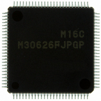
M30626FJPGP#U3C Renesas Electronics America, M30626FJPGP#U3C Datasheet - Page 204

M30626FJPGP#U3C
Manufacturer Part Number
M30626FJPGP#U3C
Description
IC M16C MCU FLASH 512K 100LQFP
Manufacturer
Renesas Electronics America
Series
M16C™ M16C/60r
Datasheets
1.QSK-62P_PLUS.pdf
(103 pages)
2.M30622SAFPU5.pdf
(308 pages)
3.M30620SPGPU3C.pdf
(423 pages)
Specifications of M30626FJPGP#U3C
Core Processor
M16C/60
Core Size
16-Bit
Speed
24MHz
Connectivity
I²C, IEBus, UART/USART
Peripherals
DMA, WDT
Number Of I /o
85
Program Memory Size
512KB (512K x 8)
Program Memory Type
FLASH
Ram Size
31K x 8
Voltage - Supply (vcc/vdd)
2.7 V ~ 5.5 V
Data Converters
A/D 26x10b; D/A 2x8b
Oscillator Type
Internal
Operating Temperature
-40°C ~ 85°C
Package / Case
100-LQFP
For Use With
867-1000 - KIT QUICK START RENESAS 62PR0K33062PS001BE - R0K33062P STARTER KITR0K33062PS000BE - KIT EVAL STARTER FOR M16C/62PM3062PT3-CPE-3 - EMULATOR COMPACT M16C/62P/30P
Lead Free Status / RoHS Status
Lead free / RoHS Compliant
Eeprom Size
-
Available stocks
Company
Part Number
Manufacturer
Quantity
Price
- Current page: 204 of 423
- Download datasheet (5Mb)
M16C/62P Group (M16C/62P, M16C/62PT)
Rev.2.41
REJ09B0185-0241
Figure 17.11
UARTi special mode register 3 (i=0 to 2)
UARTi Special Mode Register 2 (i=0 to 2)
b7 b6 b5 b4 b3 b2 b1
NOTES :
b7 b6 b5 b4
1.
2.
The DL2 to DL0 bits are used to generate a delay in SDAi output by digital means during I
mode, set these bits to “000b” (no delay).
The amount of delay varies w ith the load on SCLi and SDAi pins. Also, w hen using an external clock, the amount of
delay increases by about 100 ns.
Jan 10, 2006
b3 b2 b1 b0
UiSMR2 and UiSMR3 Registers
b0
U0SMR3 to U2SMR3
Bit Symbol
Bit Symbol
U0SMR2 to U2SMR2
NODC
SWC2
STAC
CKPH
IICM2
SWC
ALS
SDHI
(b0)
(b2)
(b4)
DL0
DL1
DL2
CSC
(b7)
—
—
—
—
Page 187 of 390
Symbol
Symbol
Nothing is assigned.
When w rite, set to “0”. When read, its content is indeterminate.
Clock Phase Set Bit
Nothing is assigned.
When w rite, set to “0”. When read, its content is indeterminate.
Clock Output Select Bit
Nothing is assigned.
When w rite, set to “0”. When read, its content is indeterminate.
SDAi Digital Delay
Setup Bit
I
Clock-Synchronous Bit
SCL Wait Output Bit
SDA Output Stop Bit
UARTi Initialization Bit
SCL Wait Output Bit 2
SDA Output Disable Bit
Nothing is assigned.
When w rite, set to “0”. When read, its content is indeterminate.
2
C Mode Select Bit 2
(1, 2)
Bit Name
Bit Name
036Dh, 0371h, 0375h
036Eh, 0372h, 0376h
Address
Address
b7 b6 b5
0 0 0 : Without delay
0 0 1 : 1 to 2 cycle(s) of UiBRG count source
0 1 0 : 2 to 3 cycles of UiBRG count source
0 1 1 : 3 to 4 cycles of UiBRG count source
1 0 0 : 4 to 5 cycles of UiBRG count source
1 0 1 : 5 to 6 cycles of UiBRG count source
1 1 0 : 6 to 7 cycles of UiBRG count source
1 1 1 : 7 to 8 cycles of UiBRG count source
0 : Without clock delay
1 : With clock delay
0 : CLKi is CMOS output
1 : CLKi is N-channel open drain output
See Table 17.13 I
0 : Disabled
1 : Enabled
0 : Disabled
1 : Enabled
0 : Disabled
1 : Enabled
0 : Disabled
1 : Enabled
0: Transfer clock
1: “L” output
0: Enabled
1: Disabled (high-impedance)
Function
2
C Mode Functions
Function
2
After Reset
000X0X0Xb
C mode. In other than I
After Reset
X0000000b
17. Serial Interface
2
C
RW
RW
RW
RW
RW
RW
RW
RW
RW
RW
RW
RW
RW
RW
—
—
—
—
Related parts for M30626FJPGP#U3C
Image
Part Number
Description
Manufacturer
Datasheet
Request
R

Part Number:
Description:
KIT STARTER FOR M16C/29
Manufacturer:
Renesas Electronics America
Datasheet:

Part Number:
Description:
KIT STARTER FOR R8C/2D
Manufacturer:
Renesas Electronics America
Datasheet:

Part Number:
Description:
R0K33062P STARTER KIT
Manufacturer:
Renesas Electronics America
Datasheet:

Part Number:
Description:
KIT STARTER FOR R8C/23 E8A
Manufacturer:
Renesas Electronics America
Datasheet:

Part Number:
Description:
KIT STARTER FOR R8C/25
Manufacturer:
Renesas Electronics America
Datasheet:

Part Number:
Description:
KIT STARTER H8S2456 SHARPE DSPLY
Manufacturer:
Renesas Electronics America
Datasheet:

Part Number:
Description:
KIT STARTER FOR R8C38C
Manufacturer:
Renesas Electronics America
Datasheet:

Part Number:
Description:
KIT STARTER FOR R8C35C
Manufacturer:
Renesas Electronics America
Datasheet:

Part Number:
Description:
KIT STARTER FOR R8CL3AC+LCD APPS
Manufacturer:
Renesas Electronics America
Datasheet:

Part Number:
Description:
KIT STARTER FOR RX610
Manufacturer:
Renesas Electronics America
Datasheet:

Part Number:
Description:
KIT STARTER FOR R32C/118
Manufacturer:
Renesas Electronics America
Datasheet:

Part Number:
Description:
KIT DEV RSK-R8C/26-29
Manufacturer:
Renesas Electronics America
Datasheet:

Part Number:
Description:
KIT STARTER FOR SH7124
Manufacturer:
Renesas Electronics America
Datasheet:

Part Number:
Description:
KIT STARTER FOR H8SX/1622
Manufacturer:
Renesas Electronics America
Datasheet:

Part Number:
Description:
KIT DEV FOR SH7203
Manufacturer:
Renesas Electronics America
Datasheet:


