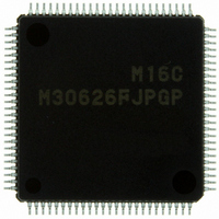
M30626FJPGP#U3C Renesas Electronics America, M30626FJPGP#U3C Datasheet - Page 247

M30626FJPGP#U3C
Manufacturer Part Number
M30626FJPGP#U3C
Description
IC M16C MCU FLASH 512K 100LQFP
Manufacturer
Renesas Electronics America
Series
M16C™ M16C/60r
Datasheets
1.QSK-62P_PLUS.pdf
(103 pages)
2.M30622SAFPU5.pdf
(308 pages)
3.M30620SPGPU3C.pdf
(423 pages)
Specifications of M30626FJPGP#U3C
Core Processor
M16C/60
Core Size
16-Bit
Speed
24MHz
Connectivity
I²C, IEBus, UART/USART
Peripherals
DMA, WDT
Number Of I /o
85
Program Memory Size
512KB (512K x 8)
Program Memory Type
FLASH
Ram Size
31K x 8
Voltage - Supply (vcc/vdd)
2.7 V ~ 5.5 V
Data Converters
A/D 26x10b; D/A 2x8b
Oscillator Type
Internal
Operating Temperature
-40°C ~ 85°C
Package / Case
100-LQFP
For Use With
867-1000 - KIT QUICK START RENESAS 62PR0K33062PS001BE - R0K33062P STARTER KITR0K33062PS000BE - KIT EVAL STARTER FOR M16C/62PM3062PT3-CPE-3 - EMULATOR COMPACT M16C/62P/30P
Lead Free Status / RoHS Status
Lead free / RoHS Compliant
Eeprom Size
-
Available stocks
Company
Part Number
Manufacturer
Quantity
Price
- Current page: 247 of 423
- Download datasheet (5Mb)
M16C/62P Group (M16C/62P, M16C/62PT)
Rev.2.41
REJ09B0185-0241
Table 17.20
NOTES:
Transfer Data Format
Transfer Clock
Transmission/Reception
Start Condition
Interrupt Request
Generation Timing
CLKi Pin Function
SOUTi Pin Function
SINi Pin Function
Select Function
1. To set SMi6 bit to “0” (external clock), follow the procedure described below.
2. Unlike UART0 to UART2, SI/Oi (i = 3 to 4) is not separated between the transfer register and buffer.
3. When SMi6 bit = 1 (internal clock), SOUTi retains the last data for a 1/2 transfer clock period after
4. When the SMi6 bit = 1 (internal clock), the transfer clock stops in the high state if the SMi4 bit = 0, or
•
•
•
Therefore, do not write the next transmit data to the SiTRR register during transmission.
completion of transfer and, thereafter, goes to a high-impedance state. However, if transmit data is
written to the SiTRR register during this period, SOUTi immediately goes to a high-impedance state,
with the data hold time thereby reduced.
stops in the low state if the SMi4 bit = 1.
If the SMi4 bit = 0, write transmit data to the SiTRR register while input on the CLKi pin is high. The
same applies when rewriting the SMi7 bit in the SiC register.
If the SMi4 bit = 1, write transmit data to the SiTRR register while input on the CLKi pin is low. The
same applies when rewriting the SMi7 bit.
Because shift operation continues as long as the transfer clock is supplied to the SI/Oi circuit, stop
the transfer clock after supplying eight pulses. If the SMi6 bit = 1 (internal clock), the transfer clock
automatically stops.
Jan 10, 2006
Item
SI/O3 and SI/O4 Specifications
Page 230 of 390
• Transfer data length: 8 bits
• SMi6 bit in SiC (i=3, 4) register = 1 (internal clock) : fj/ (2(n+1))
• SMi6 bit = 0 (external clock) : Input from CLKi pin
• Before transmission/reception can start, meet the following requirements
• When SMi4 bit in SiC register = 0
I/O port, transfer clock input, transfer clock output
I/O port, transmit data output, high-impedance
I/O port, receive data input
• LSB first or MSB first selection
• Function for setting an SOUTi initial value set function
• CLK polarity selection
fj = f1SIO, f8SIO, f32SIO. n = Setting value of SiBRG register 00h to FFh.
Write transmit data to the SiTRR register
The rising edge of the last transfer clock pulse
When SMi4 = 1
The falling edge of the last transfer clock pulse
Whether to start sending/receiving data beginning with bit 0 or beginning with
bit 7 can be selected
When the SMi6 bit in the SiC register = 0 (external clock), the SOUTi pin output
level while not transmitting can be selected.
Whether transmit data is output/input timing at the rising edge or falling edge
of transfer clock can be selected.
Specification
(2, 3)
(4)
(4)
(1)
17. Serial Interface
Related parts for M30626FJPGP#U3C
Image
Part Number
Description
Manufacturer
Datasheet
Request
R

Part Number:
Description:
KIT STARTER FOR M16C/29
Manufacturer:
Renesas Electronics America
Datasheet:

Part Number:
Description:
KIT STARTER FOR R8C/2D
Manufacturer:
Renesas Electronics America
Datasheet:

Part Number:
Description:
R0K33062P STARTER KIT
Manufacturer:
Renesas Electronics America
Datasheet:

Part Number:
Description:
KIT STARTER FOR R8C/23 E8A
Manufacturer:
Renesas Electronics America
Datasheet:

Part Number:
Description:
KIT STARTER FOR R8C/25
Manufacturer:
Renesas Electronics America
Datasheet:

Part Number:
Description:
KIT STARTER H8S2456 SHARPE DSPLY
Manufacturer:
Renesas Electronics America
Datasheet:

Part Number:
Description:
KIT STARTER FOR R8C38C
Manufacturer:
Renesas Electronics America
Datasheet:

Part Number:
Description:
KIT STARTER FOR R8C35C
Manufacturer:
Renesas Electronics America
Datasheet:

Part Number:
Description:
KIT STARTER FOR R8CL3AC+LCD APPS
Manufacturer:
Renesas Electronics America
Datasheet:

Part Number:
Description:
KIT STARTER FOR RX610
Manufacturer:
Renesas Electronics America
Datasheet:

Part Number:
Description:
KIT STARTER FOR R32C/118
Manufacturer:
Renesas Electronics America
Datasheet:

Part Number:
Description:
KIT DEV RSK-R8C/26-29
Manufacturer:
Renesas Electronics America
Datasheet:

Part Number:
Description:
KIT STARTER FOR SH7124
Manufacturer:
Renesas Electronics America
Datasheet:

Part Number:
Description:
KIT STARTER FOR H8SX/1622
Manufacturer:
Renesas Electronics America
Datasheet:

Part Number:
Description:
KIT DEV FOR SH7203
Manufacturer:
Renesas Electronics America
Datasheet:


