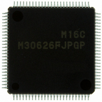
M30626FJPGP#U3C Renesas Electronics America, M30626FJPGP#U3C Datasheet - Page 265

M30626FJPGP#U3C
Manufacturer Part Number
M30626FJPGP#U3C
Description
IC M16C MCU FLASH 512K 100LQFP
Manufacturer
Renesas Electronics America
Series
M16C™ M16C/60r
Datasheets
1.QSK-62P_PLUS.pdf
(103 pages)
2.M30622SAFPU5.pdf
(308 pages)
3.M30620SPGPU3C.pdf
(423 pages)
Specifications of M30626FJPGP#U3C
Core Processor
M16C/60
Core Size
16-Bit
Speed
24MHz
Connectivity
I²C, IEBus, UART/USART
Peripherals
DMA, WDT
Number Of I /o
85
Program Memory Size
512KB (512K x 8)
Program Memory Type
FLASH
Ram Size
31K x 8
Voltage - Supply (vcc/vdd)
2.7 V ~ 5.5 V
Data Converters
A/D 26x10b; D/A 2x8b
Oscillator Type
Internal
Operating Temperature
-40°C ~ 85°C
Package / Case
100-LQFP
For Use With
867-1000 - KIT QUICK START RENESAS 62PR0K33062PS001BE - R0K33062P STARTER KITR0K33062PS000BE - KIT EVAL STARTER FOR M16C/62PM3062PT3-CPE-3 - EMULATOR COMPACT M16C/62P/30P
Lead Free Status / RoHS Status
Lead free / RoHS Compliant
Eeprom Size
-
Available stocks
Company
Part Number
Manufacturer
Quantity
Price
- Current page: 265 of 423
- Download datasheet (5Mb)
M16C/62P Group (M16C/62P, M16C/62PT)
Rev.2.41
REJ09B0185-0241
18.2
Figure 18.10
18.2.1
18.2.2
18.2.3
18.2.4
The desired resolution can be selected using the BITS bit in the ADCON1 register. If the BITS bit is set to “1”
(10-bit conversion accuracy), the A/D conversion result is stored in the bit 0 to bit 9 in the ADi register (i = 0 to
7). If the BITS bit is set to “0” (8-bit conversion accuracy), the A/D conversion result is stored in the bit 0 to bit
7 in the ADi register.
If the SMP bit in the ADCON2 register is set to “1” (with sample-and-hold), the conversion speed per pin is
increased to 28 φAD cycles for 8-bit resolution or 33 φAD cycles for 10-bit resolution. Sample and Hold is
effective in all operating modes. Select whether or not to use the Sample and Hold function before starting A/D
conversion.
In one-shot and repeat modes, the ANEX0 and ANEX1 pins can be used as analog input pins. Use the OPA1 to
OPA0 bits in the ADCON1 register to select whether or not use ANEX0 and ANEX1.
The A/D conversion results of ANEX0 and ANEX1 inputs are stored in the AD0 and AD1 registers,
respectively.
Multiple analog inputs can be amplified using a single external op-amp via the ANEX0 and ANEX1 pins. Set
the OPA1 to OPA0 bits in the ADCON1 register to “11b” (external op-amp connection mode). The inputs from
ANi (i = 0 to 7)
it back to the ANEX1 pin. The A/D conversion result is stored in the corresponding ADi register. The A/D
conversion speed depends on the response characteristics of the external op-amp. Figure 18.10 shows an
example of How to Connect the Pins in External Op-Amp.
Function
1. AN0_i and AN2_i can be used the same as ANi. However, if VCC2 < VCC1, do not use AN0_i and
Jan 10, 2006
Resolution Select Function
Sample and Hold
Extended Analog Input Pins
18.2.4 External Operation Amplifier (Op-Amp) Connection Mode
AN2_i as analog input pins.
External Op-Amp Connection
External Op-Amp
(1)
are output from the ANEX0 pin. Amplify this output with an external op-amp before sending
Page 248 of 390
ANEX1
AN0_0
AN0_1
AN0_2
AN0_3
AN0_4
AN0_5
AN0_6
AN0_7
AN2_0
AN2_1
AN2_2
AN2_3
AN2_4
AN2_5
AN2_6
AN2_7
ANEX0
AN0
AN1
AN2
AN3
AN4
AN5
AN6
AN7
ADGSEL1 to ADGSEL0 bits in ADCON2 register = 00b
ADGSEL1 to ADGSEL0 bits = 10b
ADGSEL1 to ADGSEL0 bits = 11b
Successive conversion
Resistor ladder
register
Microcomputer
Comparator
18. A/D Converter
Related parts for M30626FJPGP#U3C
Image
Part Number
Description
Manufacturer
Datasheet
Request
R

Part Number:
Description:
KIT STARTER FOR M16C/29
Manufacturer:
Renesas Electronics America
Datasheet:

Part Number:
Description:
KIT STARTER FOR R8C/2D
Manufacturer:
Renesas Electronics America
Datasheet:

Part Number:
Description:
R0K33062P STARTER KIT
Manufacturer:
Renesas Electronics America
Datasheet:

Part Number:
Description:
KIT STARTER FOR R8C/23 E8A
Manufacturer:
Renesas Electronics America
Datasheet:

Part Number:
Description:
KIT STARTER FOR R8C/25
Manufacturer:
Renesas Electronics America
Datasheet:

Part Number:
Description:
KIT STARTER H8S2456 SHARPE DSPLY
Manufacturer:
Renesas Electronics America
Datasheet:

Part Number:
Description:
KIT STARTER FOR R8C38C
Manufacturer:
Renesas Electronics America
Datasheet:

Part Number:
Description:
KIT STARTER FOR R8C35C
Manufacturer:
Renesas Electronics America
Datasheet:

Part Number:
Description:
KIT STARTER FOR R8CL3AC+LCD APPS
Manufacturer:
Renesas Electronics America
Datasheet:

Part Number:
Description:
KIT STARTER FOR RX610
Manufacturer:
Renesas Electronics America
Datasheet:

Part Number:
Description:
KIT STARTER FOR R32C/118
Manufacturer:
Renesas Electronics America
Datasheet:

Part Number:
Description:
KIT DEV RSK-R8C/26-29
Manufacturer:
Renesas Electronics America
Datasheet:

Part Number:
Description:
KIT STARTER FOR SH7124
Manufacturer:
Renesas Electronics America
Datasheet:

Part Number:
Description:
KIT STARTER FOR H8SX/1622
Manufacturer:
Renesas Electronics America
Datasheet:

Part Number:
Description:
KIT DEV FOR SH7203
Manufacturer:
Renesas Electronics America
Datasheet:


