M30626FJPGP#U3C Renesas Electronics America, M30626FJPGP#U3C Datasheet - Page 393
M30626FJPGP#U3C
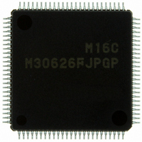
Manufacturer Part Number
M30626FJPGP#U3C
Description
IC M16C MCU FLASH 512K 100LQFP
Manufacturer
Renesas Electronics America
Series
M16C™ M16C/60r
Datasheets
1.QSK-62P_PLUS.pdf
(103 pages)
2.M30622SAFPU5.pdf
(308 pages)
3.M30620SPGPU3C.pdf
(423 pages)
Specifications of M30626FJPGP#U3C
Core Processor
M16C/60
Core Size
16-Bit
Speed
24MHz
Connectivity
I²C, IEBus, UART/USART
Peripherals
DMA, WDT
Number Of I /o
85
Program Memory Size
512KB (512K x 8)
Program Memory Type
FLASH
Ram Size
31K x 8
Voltage - Supply (vcc/vdd)
2.7 V ~ 5.5 V
Data Converters
A/D 26x10b; D/A 2x8b
Oscillator Type
Internal
Operating Temperature
-40°C ~ 85°C
Package / Case
100-LQFP
For Use With
867-1000 - KIT QUICK START RENESAS 62PR0K33062PS001BE - R0K33062P STARTER KITR0K33062PS000BE - KIT EVAL STARTER FOR M16C/62PM3062PT3-CPE-3 - EMULATOR COMPACT M16C/62P/30P
Lead Free Status / RoHS Status
Lead free / RoHS Compliant
Eeprom Size
-
Available stocks
Company
Part Number
Manufacturer
Quantity
Price


M16C/62P Group (M16C/62P, M16C/62PT)
Rev.2.41
REJ09B0185-0241
If VCC2 < VCC1, do not use AN0_0 to AN0_7 and AN2_0 to AN2_7 as analog input pins.
If the CPU reads the ADi register (i = 0 to 7) at the same time the conversion result is stored in the ADi register
after completion of A/D conversion, an incorrect value may be stored in the ADi register. This problem occurs
when a divide-by-n clock derived from the main clock or a subclock is selected for CPU clock.
If A/D conversion is forcibly terminated while in progress by setting the ADST bit in the ADCON0 register to “0”
(A/D conversion halted), the conversion result of the A/D converter is indeterminate. The contents of ADi registers
irrelevant to A/D conversion may also become indeterminate. If while A/D conversion is underway the ADST bit is
cleared to “0” in a program, ignore the values of all ADi registers.
When setting the ADST bit in the ADCON0 register to “0” in single-sweep mode during A/D conversion and
suspending A/D conversion, disable the interrupt before setting the ADST bit to “0”.
The applied intermediate potential may cause more increase in power consumption than other analog input pins
(AN0 to AN3, AN0_0 to AN0_7 and AN2_0 to AN2_7), since the AN4 to AN7 are used with the KI0 to KI3.
•
•
When operating in one-shot or single-sweep mode
When operating in repeat mode or repeat sweep mode 0 or 1
Jan 10, 2006
Check to see that A/D conversion is completed before reading the target ADi register. (Check the IR bit in
the ADIC register to see if A/D conversion is completed.)
Use the main clock for CPU clock directly without dividing it.
Page 376 of 390
24. Precautions
Related parts for M30626FJPGP#U3C
Image
Part Number
Description
Manufacturer
Datasheet
Request
R

Part Number:
Description:
KIT STARTER FOR M16C/29
Manufacturer:
Renesas Electronics America
Datasheet:

Part Number:
Description:
KIT STARTER FOR R8C/2D
Manufacturer:
Renesas Electronics America
Datasheet:

Part Number:
Description:
R0K33062P STARTER KIT
Manufacturer:
Renesas Electronics America
Datasheet:

Part Number:
Description:
KIT STARTER FOR R8C/23 E8A
Manufacturer:
Renesas Electronics America
Datasheet:

Part Number:
Description:
KIT STARTER FOR R8C/25
Manufacturer:
Renesas Electronics America
Datasheet:

Part Number:
Description:
KIT STARTER H8S2456 SHARPE DSPLY
Manufacturer:
Renesas Electronics America
Datasheet:

Part Number:
Description:
KIT STARTER FOR R8C38C
Manufacturer:
Renesas Electronics America
Datasheet:

Part Number:
Description:
KIT STARTER FOR R8C35C
Manufacturer:
Renesas Electronics America
Datasheet:

Part Number:
Description:
KIT STARTER FOR R8CL3AC+LCD APPS
Manufacturer:
Renesas Electronics America
Datasheet:
Part Number:
Description:
KIT STARTER FOR RX610
Manufacturer:
Renesas Electronics America
Datasheet:

Part Number:
Description:
KIT STARTER FOR R32C/118
Manufacturer:
Renesas Electronics America
Datasheet:

Part Number:
Description:
KIT DEV RSK-R8C/26-29
Manufacturer:
Renesas Electronics America
Datasheet:

Part Number:
Description:
KIT STARTER FOR SH7124
Manufacturer:
Renesas Electronics America
Datasheet:

Part Number:
Description:
KIT STARTER FOR H8SX/1622
Manufacturer:
Renesas Electronics America
Datasheet:

Part Number:
Description:
KIT DEV FOR SH7203
Manufacturer:
Renesas Electronics America
Datasheet: