M30626FJPGP#U3C Renesas Electronics America, M30626FJPGP#U3C Datasheet - Page 66
M30626FJPGP#U3C
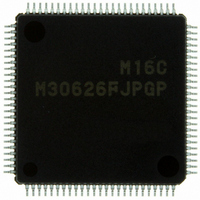
Manufacturer Part Number
M30626FJPGP#U3C
Description
IC M16C MCU FLASH 512K 100LQFP
Manufacturer
Renesas Electronics America
Series
M16C™ M16C/60r
Datasheets
1.QSK-62P_PLUS.pdf
(103 pages)
2.M30622SAFPU5.pdf
(308 pages)
3.M30620SPGPU3C.pdf
(423 pages)
Specifications of M30626FJPGP#U3C
Core Processor
M16C/60
Core Size
16-Bit
Speed
24MHz
Connectivity
I²C, IEBus, UART/USART
Peripherals
DMA, WDT
Number Of I /o
85
Program Memory Size
512KB (512K x 8)
Program Memory Type
FLASH
Ram Size
31K x 8
Voltage - Supply (vcc/vdd)
2.7 V ~ 5.5 V
Data Converters
A/D 26x10b; D/A 2x8b
Oscillator Type
Internal
Operating Temperature
-40°C ~ 85°C
Package / Case
100-LQFP
For Use With
867-1000 - KIT QUICK START RENESAS 62PR0K33062PS001BE - R0K33062P STARTER KITR0K33062PS000BE - KIT EVAL STARTER FOR M16C/62PM3062PT3-CPE-3 - EMULATOR COMPACT M16C/62P/30P
Lead Free Status / RoHS Status
Lead free / RoHS Compliant
Eeprom Size
-
Available stocks
Company
Part Number
Manufacturer
Quantity
Price


M16C/62P Group (M16C/62P, M16C/62PT)
Rev.2.41
REJ09B0185-0241
6.1
Table 6.1
Table 6.2
Normal Operating
If the D40 bit in the D4INT register is set to “1” (low voltage detection interrupt enabled), the low voltage detection
interrupt request is generated when the voltage applied to the VCC1 pin is above or below Vdet4.
The low voltage detection interrupt shares the same interrupt vector with the watchdog timer interrupt and
oscillation stop, re-oscillation detection interrupt.
Set the D41 bit in the D4INT register to “1” (enabled) to use the low voltage detection interrupt to exit stop mode.
The D42 bit in the D4INT register is set to “1” as soon as the voltage applied to the VCC1 pin reaches Vdet4 due to
the voltage rise and voltage drop. When the D42 bit changes “0” to “1”, the low voltage detection interrupt request
is generated. Set the D42 bit to “0” by program. However, when the D41 bit is set to “1” and the microcomputer is
in stop mode, the low voltage detection interrupt request is generated regardless of the D42 bit state if the voltage
applied to the VCC1 pin is detected to be above Vdet4. The microcomputer then exits stop mode.
Table 6.1 shows Low Voltage Detection Interrupt Request Generation Conditions.
The DF1 to DF0 bits in the D4INT register determine the sampling period that detects the voltage applied to the
VCC1 pin reaches Vdet4. Table 6.2 shows the Sampling Periods.
(D4INT clock)
Operating Mode
CPU Clock
1. The status except the wait mode and stop mode is handled as the normal mode. (Refer to 10. Clock
2. Refer to 6.2 Limitations on Exiting Stop Mode, 6.3 Limitations on Exiting Wait Mode.
3. An interrupt request for voltage reduction is generated a sampling time after the value of the VC13
Wait Mode
Stop Mode
(MHz)
16
Mode
Generation Circuit)
bit has changed.
See the Figure 6.6 Low Voltage Detection Interrupt Generation Circuit Operation Example for
details.
Low Voltage Detection Interrupt
Jan 10, 2006
(1)
Low Voltage Detection Interrupt Request Generation Conditions
Sampling Periods
(2)
(2)
(CPU clock divided by 8)
DF1 to DF0=00
VC27 Bit
Page 49 of 390
3.0
1
D40 Bit
(CPU clock divided by 16)
1
DF1 to DF0=01
6.0
Sampling Clock (µs)
D41 Bit
−
−
1
(CPU clock divided by 32)
DF1 to DF0=10
D42 Bit
0 to 1
0 to 1
12.0
−
−
CM02 Bit
6. Voltage Detection Circuit
−
0
1
0
(CPU clock divided by 64)
DF1 to DF0=11
24.0
VC13 Bit
0 to 1
1 to 0
0 to 1
1 to 0
− : “0”or “1”
0 to 1
0 to 1
(3)
(3)
(3)
(3)
Related parts for M30626FJPGP#U3C
Image
Part Number
Description
Manufacturer
Datasheet
Request
R

Part Number:
Description:
KIT STARTER FOR M16C/29
Manufacturer:
Renesas Electronics America
Datasheet:

Part Number:
Description:
KIT STARTER FOR R8C/2D
Manufacturer:
Renesas Electronics America
Datasheet:

Part Number:
Description:
R0K33062P STARTER KIT
Manufacturer:
Renesas Electronics America
Datasheet:

Part Number:
Description:
KIT STARTER FOR R8C/23 E8A
Manufacturer:
Renesas Electronics America
Datasheet:

Part Number:
Description:
KIT STARTER FOR R8C/25
Manufacturer:
Renesas Electronics America
Datasheet:

Part Number:
Description:
KIT STARTER H8S2456 SHARPE DSPLY
Manufacturer:
Renesas Electronics America
Datasheet:

Part Number:
Description:
KIT STARTER FOR R8C38C
Manufacturer:
Renesas Electronics America
Datasheet:

Part Number:
Description:
KIT STARTER FOR R8C35C
Manufacturer:
Renesas Electronics America
Datasheet:

Part Number:
Description:
KIT STARTER FOR R8CL3AC+LCD APPS
Manufacturer:
Renesas Electronics America
Datasheet:
Part Number:
Description:
KIT STARTER FOR RX610
Manufacturer:
Renesas Electronics America
Datasheet:

Part Number:
Description:
KIT STARTER FOR R32C/118
Manufacturer:
Renesas Electronics America
Datasheet:

Part Number:
Description:
KIT DEV RSK-R8C/26-29
Manufacturer:
Renesas Electronics America
Datasheet:

Part Number:
Description:
KIT STARTER FOR SH7124
Manufacturer:
Renesas Electronics America
Datasheet:

Part Number:
Description:
KIT STARTER FOR H8SX/1622
Manufacturer:
Renesas Electronics America
Datasheet:

Part Number:
Description:
KIT DEV FOR SH7203
Manufacturer:
Renesas Electronics America
Datasheet: