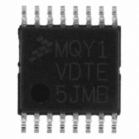
MC68HC908QY1VDTE Freescale Semiconductor, MC68HC908QY1VDTE Datasheet - Page 97

MC68HC908QY1VDTE
Manufacturer Part Number
MC68HC908QY1VDTE
Description
IC MCU 1.5K FLASH 16-TSSOP
Manufacturer
Freescale Semiconductor
Series
HC08r
Datasheet
1.MC908QY4MDWER.pdf
(184 pages)
Specifications of MC68HC908QY1VDTE
Core Processor
HC08
Core Size
8-Bit
Speed
8MHz
Peripherals
LVD, POR, PWM
Number Of I /o
13
Program Memory Size
1.5KB (1.5K x 8)
Program Memory Type
FLASH
Ram Size
128 x 8
Voltage - Supply (vcc/vdd)
2.7 V ~ 5.5 V
Oscillator Type
Internal
Operating Temperature
-40°C ~ 105°C
Package / Case
16-TSSOP
Processor Series
HC08Q
Core
HC08
Data Bus Width
8 bit
Data Ram Size
128 B
Maximum Clock Frequency
8 MHz
Number Of Programmable I/os
14
Number Of Timers
2
Maximum Operating Temperature
+ 105 C
Mounting Style
SMD/SMT
Development Tools By Supplier
FSICEBASE, M68CBL05AE, DEMO908QB8, DEMO908QC16
Minimum Operating Temperature
- 40 C
Lead Free Status / RoHS Status
Lead free / RoHS Compliant
Eeprom Size
-
Data Converters
-
Connectivity
-
Lead Free Status / Rohs Status
Details
- Current page: 97 of 184
- Download datasheet (2Mb)
Chapter 12
Input/Output Ports (PORTS)
12.1 Introduction
The MC68HC908QT1, MC68HC908QT2, and MC68HC908QT4 have five bidirectional input-output (I/O)
pins and one input only pin. The MC68HC908QY1, MC68HC908QY2, and MC68HC908QY4 have
thirteen bidirectional pins and one input only pin. All I/O pins are programmable as inputs or outputs.
12.2 Port A
Port A is a 6-bit special function port that shares all six of its pins with the keyboard interrupt (KBI) module
(see
device if the corresponding port pin is configured as an input port.
Freescale Semiconductor
Chapter 9 Keyboard Interrupt Module
Connect any unused I/O pins to an appropriate logic level, either V
Although the I/O ports do not require termination for proper operation,
termination reduces excess current consumption and the possibility of
electrostatic damage.
8-pin devices have non-bonded pins. These pins should be configured
either as outputs driving low or high, or as inputs with internal pullups
enabled. Configuring these non-bonded pins in this manner will prevent any
excess current consumption caused by floating inputs.
PTA2 is input only.
When the IRQ function is enabled in the configuration register 2
(CONFIG2), bit 2 of the port A data register (PTA) will always read a 0. In
this case, the BIH and BIL instructions can be used to read the logic level
on the PTA2 pin. When the IRQ function is disabled, these instructions will
behave as if the PTA2 pin is a logic 1. However, reading bit 2 of PTA will
read the actual logic level on the pin.
MC68HC908QY/QT Family Data Sheet, Rev. 6
(KBI)). Each port A pin also has a software configurable pullup
NOTE
NOTE
DD
or V
SS
.
97
Related parts for MC68HC908QY1VDTE
Image
Part Number
Description
Manufacturer
Datasheet
Request
R
Part Number:
Description:
Manufacturer:
Freescale Semiconductor, Inc
Datasheet:
Part Number:
Description:
Manufacturer:
Freescale Semiconductor, Inc
Datasheet:
Part Number:
Description:
Manufacturer:
Freescale Semiconductor, Inc
Datasheet:
Part Number:
Description:
Manufacturer:
Freescale Semiconductor, Inc
Datasheet:
Part Number:
Description:
Manufacturer:
Freescale Semiconductor, Inc
Datasheet:
Part Number:
Description:
Manufacturer:
Freescale Semiconductor, Inc
Datasheet:
Part Number:
Description:
Manufacturer:
Freescale Semiconductor, Inc
Datasheet:
Part Number:
Description:
Manufacturer:
Freescale Semiconductor, Inc
Datasheet:
Part Number:
Description:
Manufacturer:
Freescale Semiconductor, Inc
Datasheet:
Part Number:
Description:
Manufacturer:
Freescale Semiconductor, Inc
Datasheet:
Part Number:
Description:
Manufacturer:
Freescale Semiconductor, Inc
Datasheet:
Part Number:
Description:
Manufacturer:
Freescale Semiconductor, Inc
Datasheet:
Part Number:
Description:
Manufacturer:
Freescale Semiconductor, Inc
Datasheet:
Part Number:
Description:
Manufacturer:
Freescale Semiconductor, Inc
Datasheet:
Part Number:
Description:
Manufacturer:
Freescale Semiconductor, Inc
Datasheet:


