MC908LJ24CPKE Freescale Semiconductor, MC908LJ24CPKE Datasheet - Page 346
MC908LJ24CPKE
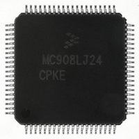
Manufacturer Part Number
MC908LJ24CPKE
Description
IC MCU 8BIT 24K FLASH 80-LQFP
Manufacturer
Freescale Semiconductor
Series
HC08r
Datasheet
1.MC908LK24CFUE.pdf
(464 pages)
Specifications of MC908LJ24CPKE
Core Processor
HC08
Core Size
8-Bit
Speed
8MHz
Connectivity
I²C, IRSCI, SPI
Peripherals
LCD, LVD, POR, PWM
Number Of I /o
48
Program Memory Size
24KB (24K x 8)
Program Memory Type
FLASH
Ram Size
768 x 8
Voltage - Supply (vcc/vdd)
3 V ~ 5.5 V
Data Converters
A/D 6x10b
Oscillator Type
Internal
Operating Temperature
-40°C ~ 85°C
Package / Case
80-LQFP
Lead Free Status / RoHS Status
Lead free / RoHS Compliant
Eeprom Size
-
Available stocks
Company
Part Number
Manufacturer
Quantity
Price
Company:

Part Number:
MC908LJ24CPKE
Manufacturer:
Freescale Semiconductor
Quantity:
10 000


Analog-to-Digital Converter (ADC)
16.8.3 ADC Clock Control Register
Data Sheet
346
Address:
The ADC clock control register (ADCLK) selects the clock frequency for
the ADC.
ADIV[2:0] — ADC Clock Prescaler Bits
ADICLK — ADC Input Clock Select Bit
Reset:
Read:
Write:
ADIV2, ADIV1, and ADIV0 form a 3-bit field which selects the divide
ratio used by the ADC to generate the internal ADC clock.
Table 16-2
should be set to between 32kHz and 2MHz.
ADICLK selects either bus clock or CGMXCLK as the input clock
source to generate the internal ADC clock. Reset selects CGMXCLK
as the ADC clock source.
ADIV2
Figure 16-9. ADC Clock Control Register (ADCLK)
$003F
ADIV2
X = don’t care
Analog-to-Digital Converter (ADC)
0
0
0
0
0
1
shows the available clock configurations. The ADC clock
= Unimplemented
ADIV1
Table 16-2. ADC Clock Divide Ratio
0
ADIV1
X
0
0
1
1
ADIV0
0
ADIV0
X
0
1
0
1
ADICLK
0
MODE1
ADC input clock ÷ 1
ADC input clock ÷ 2
ADC input clock ÷ 4
ADC input clock ÷ 8
ADC input clock ÷ 16
MC68HC908LJ24/LK24 — Rev. 2.1
R
0
ADC Clock Rate
= Reserved
MODE0
Freescale Semiconductor
1
0
0
R
0
0
Related parts for MC908LJ24CPKE
Image
Part Number
Description
Manufacturer
Datasheet
Request
R

Part Number:
Description:
Manufacturer:
Freescale Semiconductor, Inc
Datasheet:
Part Number:
Description:
Manufacturer:
Freescale Semiconductor, Inc
Datasheet:
Part Number:
Description:
Manufacturer:
Freescale Semiconductor, Inc
Datasheet:
Part Number:
Description:
Manufacturer:
Freescale Semiconductor, Inc
Datasheet:
Part Number:
Description:
Manufacturer:
Freescale Semiconductor, Inc
Datasheet:
Part Number:
Description:
Manufacturer:
Freescale Semiconductor, Inc
Datasheet:
Part Number:
Description:
Manufacturer:
Freescale Semiconductor, Inc
Datasheet:
Part Number:
Description:
Manufacturer:
Freescale Semiconductor, Inc
Datasheet:
Part Number:
Description:
Manufacturer:
Freescale Semiconductor, Inc
Datasheet:
Part Number:
Description:
Manufacturer:
Freescale Semiconductor, Inc
Datasheet:
Part Number:
Description:
Manufacturer:
Freescale Semiconductor, Inc
Datasheet:
Part Number:
Description:
Manufacturer:
Freescale Semiconductor, Inc
Datasheet:
Part Number:
Description:
Manufacturer:
Freescale Semiconductor, Inc
Datasheet:
Part Number:
Description:
Manufacturer:
Freescale Semiconductor, Inc
Datasheet:
Part Number:
Description:
Manufacturer:
Freescale Semiconductor, Inc
Datasheet: