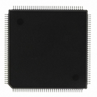
HD6417041AVF16V Renesas Electronics America, HD6417041AVF16V Datasheet - Page 36

HD6417041AVF16V
Manufacturer Part Number
HD6417041AVF16V
Description
IC SUPERH MCU ROMLESS 144QFP
Manufacturer
Renesas Electronics America
Series
SuperH® SH7040r
Specifications of HD6417041AVF16V
Core Processor
SH-2
Core Size
32-Bit
Speed
28.7MHz
Connectivity
EBI/EMI, SCI
Peripherals
DMA, POR, PWM, WDT
Number Of I /o
98
Program Memory Type
ROMless
Ram Size
4K x 8
Voltage - Supply (vcc/vdd)
3 V ~ 3.6 V
Data Converters
A/D 8x10b
Oscillator Type
Internal
Operating Temperature
-20°C ~ 75°C
Package / Case
144-QFP
Lead Free Status / RoHS Status
Lead free / RoHS Compliant
Eeprom Size
-
Program Memory Size
-
Available stocks
Company
Part Number
Manufacturer
Quantity
Price
Company:
Part Number:
HD6417041AVF16V
Manufacturer:
Renesas Electronics America
Quantity:
10 000
- Current page: 36 of 531
- Download datasheet (3Mb)
Section 3 Data Formats
3.5
The data format and valid data length varies with the instruction and DSP register. Instructions
that access the DSP data register fall into three categories: DSP data processing, X and Y data
transfer processing, and single data transfer processing.
3.5.1
When the A0 or A1 register is used as the source register in DSP fixed decimal point data
processing, the guard bits (32–39) are enabled. When any other register is used as the source
register (M0, M1, X0, X1, Y0, or Y1), the register data’s sign-extended portion goes to bits 32–39.
When the A0 or A1 register is used as the destination register, the guard bits (32–39) are enabled.
When any other register is used as the destination register, the resulting data’s bits 32–39 are
ignored.
DSP integer data processing is the same as DSP fixed decimal point data processing. The bottom
word (the bottom 16 bits, or bits 0–15) of the source register, however, is ignored. The bottom
word of the destination register is cleared with zeroes.
The top word (top 16 bits, or bits 16–31) of the source register for DSP logical data processing is
enabled. The bottom word and the guard bits of registers A0 and A1 are ignored. The top word of
the destination register is enabled. The bottom word and the guard bits of registers A0 and A1 are
cleared with zeroes.
3.5.2
The MOVX.W and MOVY.W instructions access the X and Y memory through the 16-bit X and
Y data buses. The part of data loaded to a register or stored from a register is the top word (bits
16–31). The bottom word is cleared with zeroes.
3.5.3
The MOVS.W and MOVS.L instructions can access any memory through the instruction data bus
(IDB). All DSP registers are connected to the IDB bus, which can serve as either the source and
destination register during a data transfer. There are two data transfer modes: word and longword.
In word mode, data is loaded to the top word of the DSP register or stored from the top word,
except for the A0G and A1G registers. In longword mode, data is loaded to the 32 bits of the DSP
register or stored from the 32 bits, except for the A0G and A1G registers.
Rev. 5.00 Jun 30, 2004 page 20 of 512
REJ09B0171-0500O
DSP Data Processing
X and Y Data Transfers
Single Data Transfers
DSP Instructions and Data Formats
Related parts for HD6417041AVF16V
Image
Part Number
Description
Manufacturer
Datasheet
Request
R

Part Number:
Description:
KIT STARTER FOR M16C/29
Manufacturer:
Renesas Electronics America
Datasheet:

Part Number:
Description:
KIT STARTER FOR R8C/2D
Manufacturer:
Renesas Electronics America
Datasheet:

Part Number:
Description:
R0K33062P STARTER KIT
Manufacturer:
Renesas Electronics America
Datasheet:

Part Number:
Description:
KIT STARTER FOR R8C/23 E8A
Manufacturer:
Renesas Electronics America
Datasheet:

Part Number:
Description:
KIT STARTER FOR R8C/25
Manufacturer:
Renesas Electronics America
Datasheet:

Part Number:
Description:
KIT STARTER H8S2456 SHARPE DSPLY
Manufacturer:
Renesas Electronics America
Datasheet:

Part Number:
Description:
KIT STARTER FOR R8C38C
Manufacturer:
Renesas Electronics America
Datasheet:

Part Number:
Description:
KIT STARTER FOR R8C35C
Manufacturer:
Renesas Electronics America
Datasheet:

Part Number:
Description:
KIT STARTER FOR R8CL3AC+LCD APPS
Manufacturer:
Renesas Electronics America
Datasheet:

Part Number:
Description:
KIT STARTER FOR RX610
Manufacturer:
Renesas Electronics America
Datasheet:

Part Number:
Description:
KIT STARTER FOR R32C/118
Manufacturer:
Renesas Electronics America
Datasheet:

Part Number:
Description:
KIT DEV RSK-R8C/26-29
Manufacturer:
Renesas Electronics America
Datasheet:

Part Number:
Description:
KIT STARTER FOR SH7124
Manufacturer:
Renesas Electronics America
Datasheet:

Part Number:
Description:
KIT STARTER FOR H8SX/1622
Manufacturer:
Renesas Electronics America
Datasheet:

Part Number:
Description:
KIT DEV FOR SH7203
Manufacturer:
Renesas Electronics America
Datasheet:


