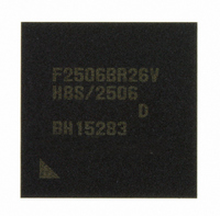
DF2506BR26DV Renesas Electronics America, DF2506BR26DV Datasheet - Page 6

DF2506BR26DV
Manufacturer Part Number
DF2506BR26DV
Description
IC H8S/2506 MCU FLASH 176-LFBGA
Manufacturer
Renesas Electronics America
Series
H8® H8S/2500r
Specifications of DF2506BR26DV
Core Processor
H8S/2000
Core Size
16-Bit
Speed
26MHz
Connectivity
I²C, SCI
Peripherals
POR, PWM, WDT
Number Of I /o
104
Program Memory Size
512KB (512K x 8)
Program Memory Type
FLASH
Ram Size
32K x 8
Voltage - Supply (vcc/vdd)
3 V ~ 5.5 V
Data Converters
A/D 16x10b; D/A 2x8b
Oscillator Type
Internal
Operating Temperature
-40°C ~ 85°C
Package / Case
176-LFBGA
Lead Free Status / RoHS Status
Lead free / RoHS Compliant
Eeprom Size
-
Available stocks
Company
Part Number
Manufacturer
Quantity
Price
Company:
Part Number:
DF2506BR26DV
Manufacturer:
Renesas Electronics America
Quantity:
10 000
5
Inheriting the respected H8 architecture and improving processing ability and speed.
High-performance CISC architecture
Based on core development focused on compatibility, the H8S Family and H8SX Family also feature upward compatibility in register
layout and functionality. This makes reuse of software resources easy. Furthermore, functions that improve ease of use are added to
each family.
Assuring compatibility at the object level
Firmware developed for the H8 CPU can be used on the 16-bit H8S CPU and the 32-bit H8SX CPU as well.
CPU register structure
H8S/2600
(H8S/2600, H8S/2400 Series)
H8S/2000
H8/300H
H8/300
H8/300L
57instructions
ER0
ER1
ER2
ER3
ER4
ER5
ER6
ER7 (SP)
PC
MAC
VBR
SBR
15
31
63
31
31
31
• Multiply and accumulate instructions
• Bit manipulation
• Improved shift instructions
• Save and restore of
• 8, 16, and 32-bit move and
• Multiply and divide instructions
(MAC, CLRMAC, LDMAC, STMAC)
multiple registers
arithmetic instructions
• Supports operations with memory
• Improved addressing modes
• Improved bit manipulation instructions
• Support for short instructions
• Expanded data bus width (from 16 to 32 bits)
• + 5
62instructions
instructions
E0
E1
E2
E3
E4
E5
E6
E7
23
(Code expansion)
• MULXS
• DIVXS
• EXTS
• EXTU
• TRAPA
65instructions
MACL
0 7
• + 3
instructions
15
R0H
R1H
R2H
R3H
R4H
R5H
R6H
R7H
• LDH
• STM
• TAS
12
CCR
EXR
8
0
• + 4
7 6 5 4 3 2 1 0
7 6 5 4 3 2 1 0
7
T
41
instructions
I UI H U N Z V C
69instructions
(Reserved)
(Reserved)
MACH
R0L
R1L
R2L
R3L
R4L
R5L
R6L
R7L
• MAC
• LDMAC
• STMAC
• CLRMAC
I2 I1 I0
32
0
0
0
0
0
• + 18
I2 to I0
CCR
MAC
instructions
EXR
VBR
SBR
SP
PC
UI
H
U
N
Z
V
C
T
I
: Stack pointer
: Program counter
: Condition code register
: Interrupt mask bit
: User bit/interrupt mask bit
: Half carry flag
: User bit
: Negative flag
: Zero flag
: Overflow flag
: Carry flag
: Extend register
: Trace bit
: Interrupt mask bits
: Multiply register
: Vector base register
: Short address base register
H8/300,300L-CPU
H8/300H-CPU
H8S/2000-CPU
H8S/2600-CPU
H8SX-CPU
87instructions
• MOVA
• MOVMD
• MOVSD
• MULU
• MULS
• DIVU
• DIVS
• RTS/L
• RTE/L
• BRA/S
• BSET/EQ
• BSET/NE
• BCLR/EQ
• BCLR/NE
• BSTZ
• BISTZ
• BFLD
• BFST
(Added)
(Added)
(Added)
(Added)
High-speed 32-bit processing
for high performance
These CPUS use a 2-stage pipelined processing plus
instruction FIFO structure to achieve high-speed processing at
one instruction per clock cycle. Furthermore, by making the
internal CPU bus 32 bits wide, the instruction fetch time is
reduced significantly from earlier 16-bit MCUs.
The H8SX inherits the whole
H8S instruction set.
In addition to inheriting the whole H8S instruction set, which is
ideal for embedded applications, the H8SX adds new
instructions and new addressing modes to improve ease of
use even further. Arithmetic performance is improved greatly
by the provision of 32-bit multiply and divide instructions.
VBR reduces the interrupt response
time significantly.
These MCUs feature a VBR (vector base register) function that
can set up an arbitrary address in a vector table. By allocating
the vector in RAM, even ROM-less versions can perform
interrupt handling quickly.
SBR creates faster programs.
The SBR (short address base register) function makes it
possible to set up a start address for an 8-bit absolute address
space at an arbitrary location. Fast and efficient programs can
be created by changing the start address of the 8-bit absolute
address space.
H8SX-CPU
Dhrystone 1.1
MIPS value
Fixed : H'000000
Fixed : H'000000
50
40
30
20
10
address
H8SX MCU
16-bit MCU
Clock
(@25MHz)
11.2MIPS
H8S/2000
VBR
8-bit absolute address space
Vector address area
Earlier systems
Earlier systems
Instruction
I/O register group
Instruction 1
SBR
1
4.5 times
Instruction decoder
ROM
RAM
ROM
RAM
Instruction
CCR, EXR
ER0-ER7
2
PC
15.1MIPS
H8S/2600
(@33MHz)
Instruction FIFO (16bit 8 )
Instruction
Instruction 2
3
Instruction
data bus
ALU
32bit
3.3 times
Instruction
4
AU
Instruction
VBR : H'xxxxxx
VBR : H'xxxxxx
Instruction 3
5
INC
H8SX/1500
(@40MHz)
40MIPS
(for new format)
These achieve
multiplier
1 MIPS/MHz
Instruction 4
8-bit absolute address space
8-bit absolute address space
About 1/2
divider
Vector address area
Vector address area
I/O register group
H8SX/1600
(@50MHz)
50MIPS
H8SX
H8SX
ROM
RAM
Instruction 5
H8SX CPU added
functionality
32bit
data bus
6


