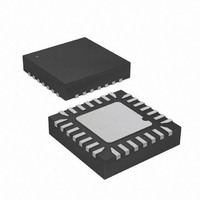
ATMEGA48V-10MMU Atmel, ATMEGA48V-10MMU Datasheet - Page 107

ATMEGA48V-10MMU
Manufacturer Part Number
ATMEGA48V-10MMU
Description
MCU AVR 4K FLASH 10MHZ 28-QFN
Manufacturer
Atmel
Series
AVR® ATmegar
Specifications of ATMEGA48V-10MMU
Core Processor
AVR
Core Size
8-Bit
Speed
10MHz
Connectivity
I²C, SPI, UART/USART
Peripherals
Brown-out Detect/Reset, POR, PWM, WDT
Number Of I /o
23
Program Memory Size
4KB (2K x 16)
Program Memory Type
FLASH
Eeprom Size
256 x 8
Ram Size
512 x 8
Voltage - Supply (vcc/vdd)
1.8 V ~ 5.5 V
Data Converters
A/D 8x10b
Oscillator Type
Internal
Operating Temperature
-40°C ~ 85°C
Package / Case
28-VQFN Exposed Pad, 28-HVQFN, 28-SQFN, 28-DHVQFN
Processor Series
ATMEGA48x
Core
AVR8
Data Bus Width
8 bit
Data Ram Size
512 B
Interface Type
2-Wire, SPI, USART, Serial
Maximum Clock Frequency
10 MHz
Number Of Programmable I/os
23
Number Of Timers
3
Maximum Operating Temperature
+ 85 C
Mounting Style
SMD/SMT
3rd Party Development Tools
EWAVR, EWAVR-BL
Minimum Operating Temperature
- 40 C
On-chip Adc
10 bit, 8 Channel
Package
28MLF EP
Device Core
AVR
Family Name
ATmega
Maximum Speed
10 MHz
Operating Supply Voltage
2.5|3.3|5 V
For Use With
ATSTK600 - DEV KIT FOR AVR/AVR32ATAVRDRAGON - KIT DRAGON 32KB FLASH MEM AVR
Lead Free Status / RoHS Status
Lead free / RoHS Compliant
Available stocks
Company
Part Number
Manufacturer
Quantity
Price
Company:
Part Number:
ATMEGA48V-10MMU
Manufacturer:
ZILOG
Quantity:
1
- Current page: 107 of 378
- Download datasheet (8Mb)
15. 16-bit Timer/Counter1 with PWM
15.1
15.2
2545S–AVR–07/10
Features
Overview
•
•
•
•
•
•
•
•
•
•
•
The 16-bit Timer/Counter unit allows accurate program execution timing (event management),
wave generation, and signal timing measurement.
Most register and bit references in this section are written in general form. A lower case “n”
replaces the Timer/Counter number, and a lower case “x” replaces the Output Compare unit
channel. However, when using the register or bit defines in a program, the precise form must be
used, that is, TCNT1 for accessing Timer/Counter1 counter value and so on.
A simplified block diagram of the 16-bit Timer/Counter is shown in
placement of I/O pins, refer to
ters, including I/O bits and I/O pins, are shown in bold. The device-specific I/O Register and bit
locations are listed in the
The PRTIM1 bit in
enable Timer/Counter1 module.
True 16-bit Design (that is, allows 16-bit PWM)
Two independent Output Compare Units
Double Buffered Output Compare Registers
One Input Capture Unit
Input Capture Noise Canceler
Clear Timer on Compare Match (Auto Reload)
Glitch-free, Phase Correct Pulse Width Modulator (PWM)
Variable PWM Period
Frequency Generator
External Event Counter
Four independent interrupt Sources (TOV1, OCF1A, OCF1B, and ICF1)
“PRR – Power Reduction Register” on page 43
“Register Description” on page
“Pinout ATmega48/88/168” on page
129.
ATmega48/88/168
2. CPU accessible I/O Regis-
Figure
must be written to zero to
15-1. For the actual
107
Related parts for ATMEGA48V-10MMU
Image
Part Number
Description
Manufacturer
Datasheet
Request
R

Part Number:
Description:
IC AVR MCU 4K 5V 10MHZ 32-TQFP
Manufacturer:
Atmel
Datasheet:

Part Number:
Description:
IC AVR MCU 4K 10MHZ 1.8V 32-QFN
Manufacturer:
Atmel
Datasheet:

Part Number:
Description:
IC AVR MCU 4K 10MHZ 1.8V 28DIP
Manufacturer:
Atmel
Datasheet:

Part Number:
Description:
IC AVR MCU 4K 5V 10MHZ 32-TQFP
Manufacturer:
Atmel
Datasheet:

Part Number:
Description:
IC AVR MCU 4K 5V 12MHZ 32-QFN
Manufacturer:
Atmel
Datasheet:

Part Number:
Description:
IC AVR MCU 4K 5V 10MHZ 32-QFN
Manufacturer:
Atmel
Datasheet:

Part Number:
Description:
IC AVR MCU 4K 5V 10MHZ 28-DIP
Manufacturer:
Atmel
Datasheet:

Part Number:
Description:
IC AVR MCU 4K 5V 10MHZ 28-DIP
Manufacturer:
Atmel
Datasheet:

Part Number:
Description:
MCU AVR 4KB FLASH 10MHZ 32TQFP
Manufacturer:
Atmel
Datasheet:

Part Number:
Description:
MCU AVR 4KB FLASH 10MHZ 32QFN
Manufacturer:
Atmel
Datasheet:

Part Number:
Description:
MCU AVR 4KB FLASH 20MHZ 28QFN
Manufacturer:
Atmel
Datasheet:


